saeedmns68
Junior Member level 1
Im making a half bridge 300v 14khz square wave power supply by using two ultra fast IGBTs and a IR2153 gate driver,when the power part of the circuit is inacvtive(Vcc=0 V) the gate-emitter waveform on high side IGBT is good with peak to peak voltage of VGE=11200mV , but when the power is activated and no load is at the output of the circuit(IC=0) the waveform will contain high frequency noise with 7000mV mixed with original waveform
 View attachment VGE HI BEFORE CONNECTING POWER VPP=11.3V.bmp peak to peak ,the power supply of high and low side VGE is two isolated L7812CV output,what can be wrong in my circuit?pls help me
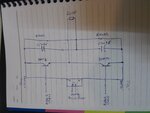
the schematic of the circuit and os screenshots are attached to the message
 View attachment VGE HI BEFORE CONNECTING POWER VPP=11.3V.bmp peak to peak ,the power supply of high and low side VGE is two isolated L7812CV output,what can be wrong in my circuit?pls help me
the schematic of the circuit and os screenshots are attached to the message