Continue to Site

Welcome to EDAboard.com

Welcome to our site! EDAboard.com is an international Electronics Discussion Forum focused on EDA software, circuits, schematics, books, theory, papers, asic, pld, 8051, DSP, Network, RF, Analog Design, PCB, Service Manuals... and a whole lot more! To participate you need to register. Registration is free. Click here to register now.

Problem with RCD circuit of flyback converter

Status
Not open for further replies.

loxly

Junior Member level 3
Joined
Mar 16, 2012
Messages
29
Helped
6
Reputation
12
Reaction score
6
Trophy points
1,283
Location
Zagreb, Croatia
Activity points
1,530
I have some questions regarding to design of RCD circuit of flyback converter.

Converter specifications:

input: 50 V
output 100 V, 100 W (100 Ohm resistance)
Output current 1 A
transformer current ripple 2A (CCM)
output capacitor 680 uF, 100 V
Turns ratio: 1
Duty cycle: 0.67

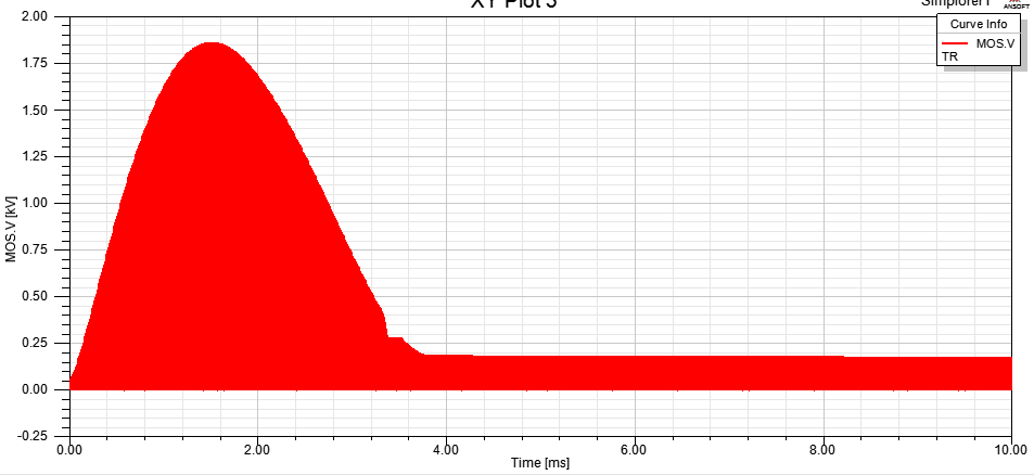
The problem is that when I'm using calculated R and C values ( according to some equations I've found 10k, 47 nF) , I still get quite large (above kV) voltage spikes on my Simplorer model simulation. But when I use a combination of quite larger value for C (47 or 150 uF) and R (33k, for smaller losses) everything seems ok on the simulation! (spikes are reasonable).

I've been searching a lot, and I haven't found anywhere that someone uses RCD snubber capacitor much larger than 47 nF!

It's maybe because of large output capacitor, but I can't change it. It is already on the board where we constructed universal non-isolated DC converter.

Are there any drawbacks of using such a large capacitor in snubber circuit? What could cause this?

I don't have anything against using such a big capacitor if you don't :)

I don't have any experience in flyback design, so I'm asking you.

Thank you for your help

Lovro

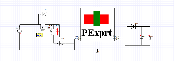
P.S. I have modeled flyback transformer in PExpert and add model in simplorer, so it's pretty accurate. I can even send you my flyback Simplorer model if needed!
 

Is this supposed to be a clamp type RCD or a slew-rate limiting RCD?
 

The snubber numbers don't sound reasonable, but we would need to know the transformer parameters (main and leakage inductance) to check it.
 

Yes, need to know the primary leakage inductance, peak primary current, and operating frequency and duty cycle to really size the snubber components.
 

Ok, here there are:

Transformer main inductance: 180 uH

Primary leakage inductance: PExprt calculated that DC value leakage inductance is 965 nH, and switching freq. value leakage inductance is 454 nH, but I would say those numbers are too small, it is maybe for perfectly wounded transformer...I would go with 3% of main inductance

Peak primary current: 3.9 A

Frequency: 100 kHz

Duty cycle: 66.67% (2/3)

Here are some other parameters just for case...

Transformer number of turns: 16 (P and H have both 16 windings, each winding is in one layer)

Core: ETD 49/25/16 (material N87, gap 0.4 mm, max B is 0.195 T, variation of B is 0.094 T)
Wire gauge: AWG 15


As I said, maybe I got such unusual values for snubber R and C because of big output capacitor (680 uH,)

I only have to construct an educational model (similar to Mohan's), it doesn't have to be optimized, it only has to work :)

Thank you guys for your support!
 

Somewhat curious how you rave about pretty accurate PExpert simulation results and then use a tenfold rule-of-thumb leakage inductance number...

However putting in your parameters in a hand calculation of stored energy, I get about 8 V overvoltage with a 47 nF snubber capacitor and 65V with 4.7 nF. The resistor has to be adjusted, because it must be able to absorb the leak inductance energy with a specified overvoltage, which is basically indepdendent of the snubber capacitance value.

With 3.9 A/5.4 uH (your 3% assumption) leakage inductance, you get 41 uWs stored energy respectively 4.1 W snubber loss, a simple calculation. But the voltage won't go much above 200 V with a 10 k discharge resistor, so your kV numbers aren't feasible.

If efficiency is an objective, you need either to reduce the leakage inductance or choose a circuit, that allows recovery of leakage inductance energy.
 
  • Like
Reactions: loxly

    loxly

    Points: 2
    Helpful Answer Positive Rating
Hi,

before you go ahead with calculations you need to know the following points:

Believe it or not, the RCD snubber circuit works like a Zener, in fact, it is called "RCD clamp circuit".


The most important component is the capacitor: the clamp component is the capacitor.


The capacitor, once charged by the diode, becomes an open circuit and no more current can flow into it.

The capacitor, once charged shows a constant voltage across its pin, just like a Zener.

The resistor is needed because the capacitor must discharge before the next PWM cycle.

The R*C time constant must be 5 to 6 times the switching time period.

The diode charges the capacitor in the very first 100/200 ns of the Toff time.


Hope that'll help :)
Enrico Migliore
 
  • Like
Reactions: loxly

    loxly

    Points: 2
    Helpful Answer Positive Rating
Ok, now I've put R=10k, C=47nF values in my snubber circuit and ran 10 ms simulation.

According to simulation, now i got 1.8 kV spikes in first 2-3 seconds of simulation, and after that voltage settles down, and the spikes are reasonable.

So actually I have a huge voltage spikes in first few seconds, and after that, everything seems ok. ( drain to source MOS voltage)

Is it maybe because of very big output C (comparing to snubber's C)? Will this be a problem for MOS?

In simulation, duty cycle is set in the very beginning, when I will be testing the real thing i will start with D=0 and then set it to 67%. Will that solve the problem?

Here is the snapshot of simulation so you can get the picture:


The normal voltage across MOS is about 150V, first few ms spikes are huge, and after that they become reasonable
 

I guess, you need to show your simulation circuit and setup. Something seems to be very different from a reasonable flyback design.
 

Here they are:

96_1333198660.png
 

Unfortunately we can't see the simulation details. My guess is that you are driving the MOSFET with constant PWM despite a discharged output capacitor. This causes the inductor current to increase beyond reasonable limits during startup. In a real circuit, the switch transistor would be immediately destroyed or the input fuse blown, but in a simulation, you can do the impossible.

Just monitor the primary current during startup. :-D

P.S.: Using a current mode controller (limiting inductor peak current) is a simple means to avoid serious overcurrent problems in a real circuit and the demonstrated kind of pseudo problems in simulation.
 
Last edited:
  • Like
Reactions: loxly

    loxly

    Points: 2
    Helpful Answer Positive Rating
Primary current during startup is about 130A, but just for the 2-3 seconds :-D

Hmm, how could I solve this enormous startup current and voltage spikes?

Maybe if I start with D=0% and then slowly increase it to 67%?

This project is becoming a real nightmare :D

I uploaded my model, so if you have Simplorer you could check it out :)

Converter should work in open-loop mode, so current or voltage controler is not an option :)
 

I don't have Simplorer and don't need it, I think, because the problem is pretty basic. You don't don't need a simulation to understand it.

Slow pwm start can help, current mode is a more general and reliable solution.
 
  • Like
Reactions: loxly

    loxly

    Points: 2
    Helpful Answer Positive Rating
Thank you very much!

I think that current mode controller would be too much for me. I have no experience at all.

I think I will take my chance with slow PWM start, and hope I won't fry anything :)

I have another questin, but this will be pretty easy to you :)

So, the losses in snubber circuit depends on leakage inductance. It means that snubber C stores energy, and all of that energy MUST be dissipated on R during off period. So actually, losses in RCD circuit depends of leakage inductance, not of R. R just have too be small enough so all the energy (power) can be dissipated on it.

Am I saying this right? :)

I'm a little bit confused because I've seen somewhere that losses in RCD circuit are calculated with dissipation on R ( U^2/R)
 

Current mode controller or at least peak current limiting isn't a big thing an can be set up in a SPICE or similar simulator circuit. But slow start (duty cycle ramp) should serve the purpose, at least under defined load conditions.

Assuming leakage inductance energy (Ipk²*Ls/2) to be balanced with resistor power dissipation has been my calculation base. It's the minimal snubber resistor power dissipation, that only applies, if the capacitor voltage stays above primary flyback voltage (ideally 100 V in your example). If you reduce the time constant, additional energy will be "burned" in the resistor.
 
  • Like
Reactions: loxly

    loxly

    Points: 2
    Helpful Answer Positive Rating
Now I get it! Leakage inductance energy times frequency is the minimal power dissipation in snubber circuit. That power must be dissipated on R. So, if R is not low enough, it's voltage increases so it can burn all the power!

Thank you very much for your time and effort, you really helped me much.

After flyback I have to create forward converter, so I'll be probably having more questions then :)

I hope I wouldn't have to bug you ever more with flyback converter, but you never know... ;)

Lovro
 

Yes, so long as the clamp capacitor voltage never goes beyond the normal flyback voltage (Vout*Np/Ns), the resistor dissipation will just be equal to leakage energy * fs.

If you can't implement some kind of soft start or current limiting, you could just try setting initial conditions on the output capacitor so it starts near its steady state voltage. Not sure if your simulation software can implement that though. I think most people on the power electronics boards are familiar with LTspice, which is excellent at SMPS simulation.
 
  • Like
Reactions: loxly

    loxly

    Points: 2
    Helpful Answer Positive Rating
I've set initial value of C to 100, and now everything seems great, no voltage or current spikes :)

Oh, now i remembered something...

When I calculate MOS dissipation I use Irms^2xRds(on) + switching losses

As I remember, diode losses are calculated with Vf x Iav (forward voltage drop times average current, in my case Iav=1A)

I need this information to calculate if cooler for diode is needed or not
 

Status
Not open for further replies.

Similar threads

Part and Inventory Search

Welcome to EDABoard.com

Sponsor

Back
Top