Continue to Site

Welcome to EDAboard.com

Welcome to our site! EDAboard.com is an international Electronics Discussion Forum focused on EDA software, circuits, schematics, books, theory, papers, asic, pld, 8051, DSP, Network, RF, Analog Design, PCB, Service Manuals... and a whole lot more! To participate you need to register. Registration is free. Click here to register now.

FPGA program has some hard to trace glitches

Status
Not open for further replies.

Saltwater

Member level 3
Joined
Aug 30, 2015
Messages
64
Helped
0
Reputation
0
Reaction score
0
Trophy points
1,286
Activity points
1,867
Hi,

I was doing some FPGA and was wondering if it's a problem on the FPGA side of things. The calculations are done using relatively high frequency and with a high data bandwith 64bit "large multipliers" and in the 20mHz range. I might have done something wrong with integer calculations..

My question was, is it likely that under some workload a Cyclone 5 FPGA starts to croak, or is it expected to have flawless performance across the board?
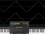

quartus.png

Kind regards,
 

Hi,

since an FPGA works as parallel machine there is no value like "workload". Either it is within timing specification or not. If it is within timing specifications, it should work.
If it is outside timing specifications: it may work, it may work part times (as in your case) or it may completely fail.

Did you properly set up your timing constraints and did you check that the design meets those requirements?

btw: 20mHz is rather slow... even 20MHz is not very fast for an FPGA. But for sure you have to take care about proper clocking / pipelining the data.


Klaus
 

As Klaus said FPGA's are much different than a processor. A peice of code compiles to physical gates inside the FPGA. Those gates are basically unaffected by anything else going on.


It's more likely you have a functional problem (like an integer rollover) or a timing problem.

Does the problem repeat with the same inputs? If yes then it's likely functional so try and simulate it. If it's random its more likely timing.

Timing is a complicated subject but make sure you've 'told' your tool what your clock frequency is. Keep the clocking as simple as possible. Ideally you have a single clock used in your always @(posedge clk) statements. When you have different clocks you need to ensure they work together properly.
 

Yes, it's in MHz, not in miliHertz. It can probably do a couple of decades tho. :grin:

Did you properly set up your timing constraints and did you check that the design meets those requirements?
Klaus


I have the most basic constraint. I use sample and hold before the DAC and everything follows the clock scheme. It's not really critically timed.
Code:
derive_pll_clocks -create_base_clocks
derive_clock_uncertainty

#create_clock -period 20 [get_ports CLOCK_50]
#create_clock -period 20 [get_ports CLOCK2_50]
#create_clock -period 20 [get_ports CLOCK3_50]
#create_clock -period 20 [get_ports CLOCK4_50]

Could well be typo's creeped in, may have to check that. Thinking if you miss math by clocking it would be all the time.
 

The only kind of "workload" that could affect the life of your Cyclone V FPGA would be running the part at a die temperatures upwards of 85C as they do in accelerated life testing.

As the other have stated check your timing.
1) verify that the design met all timing constraints.
2) verify that your timing constraints cover all paths, including input and output pins
3) If you have more than one clock, verify that you have properly crossed the clock domains

If the problem isn't in the timing after checking all the above.
4) run the design in a testbench, if you didn't do this prior to trying this out on a device, then let this be a lesson, run a simulation before you put it on a board, because the only things that work are the things you verify in simulation (seen this happen on many projects; it's simple I don't need to simulate it....guess what part of the design didn't work?).
5) if the simulation shows it should be working, the you likely have a corner case that isn't tested in simulation. Insert in system debug in the design, Intel has Signal Tap (not sure if this is an additional license) or you can run signals out to some pins you can monitor with a logic analyzer or multichannel scope.

- - - Updated - - -

Code:
derive_pll_clocks -create_base_clocks
derive_clock_uncertainty

#create_clock -period 20 [get_ports CLOCK_50]
#create_clock -period 20 [get_ports CLOCK2_50]
#create_clock -period 20 [get_ports CLOCK3_50]
#create_clock -period 20 [get_ports CLOCK4_50]

Could well be typo's creeped in, may have to check that. Thinking if you miss math by clocking it would be all the time.

In standard SDC constraint format all those statements proceeded by # are commented out. That would mean you have no input clock constraint unless there is one above the derive_pll_clocks line. Besides that, any create_clock command should be before any derive command.
 

Does the problem repeat with the same inputs? If yes then it's likely functional so try and simulate it. If it's random its more likely timing.

It's an occasional blip, it prefers the same spots though, always before or after the crest.

- - - Updated - - -

In standard SDC constraint format all those statements proceeded by # are commented out. That would mean you have no input clock constraint unless there is one above the derive_pll_clocks line. Besides that, any create_clock command should be before any derive command.

Thanks for the advice, I will try that. Thought it would'nt be needed like this.

- - - Updated - - -

Yes, it's in MHz, not in miliHertz. It can probably do a couple of decades tho. :grin:

Did you properly set up your timing constraints and did you check that the design meets those requirements?
Klaus


I have the most basic constraint. I use sample and hold before the DAC and everything follows the clock scheme. It's not really critically timed.
Code:
derive_pll_clocks -create_base_clocks
derive_clock_uncertainty

#create_clock -period 20 [get_ports CLOCK_50]
#create_clock -period 20 [get_ports CLOCK2_50]
#create_clock -period 20 [get_ports CLOCK3_50]
#create_clock -period 20 [get_ports CLOCK4_50]

Could well be typo's creeped in, may have to check that. Thinking if you miss math by clocking it would be all the time.

- - - Updated - - -

Pff simulating it is,
Still these errors presist.
sweep.jpg
 

Looking at a waveform without seeing or understanding what you're actually trying to do doesnt tell us a lot. So far, to summarise, you have asked - "My design doesnt work, whats the problem?" and so people have answered with very generic answers.
If you want specific answers, you're going to have to ask specific questions and probably post some code exhibiting the problem.
 

Finally I found my problem, it was in crossing clock domains. It goes from a higher to a lower frequency clock, and data should be present. So new to this I guess it's down to setup hold time for a given latch. I have 3 sepparate pll clocks, two of them should be at work, +1 later. Is this something I can solve using a Quartus setup "pll setup"?
 
Last edited:

Hi,

my recommendation: avoid using different clocks.

Use one (fast) system_clock and synchronize all other signals and processes to this clock.


Klaus
 

That would be simplest. The concept is I can substitute errors in math which is about 80% in some cases, with altering the frequency which is to a lesser degree subject to reflecting these errors. If there's a way it would be really cool. Given I have USB ready and waiting makes there is another domain to be crossed.
 

hi,

if you give more information, we are able to give better assistance.

Klaus
 

When I saw the original waveform I was wondering if you were crossing clock domains with a multi-bit value. That can easily result in values that go out of range when multiple bits change like incrementing from 01111 to 10000. It was the reason I had "3) If you have more than one clock, verify that you have properly crossed the clock domains" in post #5.

Unless the clocks are integer multiples of each other and phase and frequency locked you won't be able to reliably transfer multi-bit values across the clock domains, you will either have to use an asynchronous FIFO or build a clock domain crossing for the multi-bit value by holding the value to transfer static and send another single to indicate the data is static and can be captured in the other clock domain.
 

Unless the clocks are integer multiples of each other and phase and frequency locked you won't be able to reliably transfer multi-bit values across the clock domains, you will either have to use an asynchronous FIFO or build a clock domain crossing for the multi-bit value by holding the value to transfer static and send another single to indicate the data is static and can be captured in the other clock domain.

That's exactly the realization I'm having right now. I built the sample and hold to double flip flop. But it doesn't work because the clocks are mismatched to not even within an integer multiple of each other. I'm going to try and build the asynchronous FIFO, and soup up the clock so it's a multiple of 2,7306x.


Thanks!

If you use an asynchronous FIFO you don't need to ensure the clocks are integer multiples of each other. That's the whole point of using an async FIFO, otherwise why bother using a FIFO that requires more resources to implement, when a synchronous FIFO would work.
 

If you use an asynchronous FIFO you don't need to ensure the clocks are integer multiples of each other. That's the whole point of using an async FIFO, otherwise why bother using a FIFO that requires more resources to implement, when a synchronous FIFO would work.

I gave up trying this, it has become a hassle. The clocks are too close together and the signal syncing frames is the only thing I have to cause a trigger from the slow domain to the fast domain. In triggering from slow to fast the problem just shifts, and has the effect of distortion shifting from the other domain. In order to try this I used a double counter for the FIFO, so I need the sample and hold to tell both counters to go to the next index. Again double flopping did nothing.. Maybe the answer is a bigger FIFO, but I can shure use the logic it would take. Handshaking will cause the data to be semi valid which for DSP purpose is not allowed. So for this design,?
 

There are lots of ways to do this...if the clocks are known you can implement a circular buffer with a grey code counter. One side loads the buffer at the location pointed to by the counter. The other side takes from the buffer at a location a few counts away from what the counter says.

If the fast side is the one 'producing' the data you'll need to make the circular buffer multiple samples deep and make sure it increments the grey code counter at a rate slow enough to guarantee the slow side sees changes.

This solution may be somewhat inflexible in terms of clock frequencies (or requires an over-sized buffer), but avoids bidirectional handshaking.

You are describing what is already in an asynchronous FIFO, which I think the OP has said doesn't work.

It appears that the OP may not know how to deal with a fill/drain problem of FIFOs/Circular_queues without running into either over/under flows, when the fill side clock rate is high and the drain clock rate is low. They mention trying to run handshaking across the clock boundary is causing problems, which kind of tells me that they are trying to generate the output data rate based on an signal in the input clock domain.

The key in those situations is if the input data rate (not the input clock frequency) and the output data rate (not the output clock frequency) are the same and you must not drop or otherwise disturb the data then you need to decide or determine if you have burst input data or input data that comes at the specific rate (this is the major determining factor in how large the FIFO/queue is) and you need an NCO to generate the exact same output data rate as the input rate to ensure the FIFO/queue never over/underflows. If the clocks are asynchronous to each other (i.e. not generated off the same time base, e.g. from a PLL) then you will need to occasionally resynchronize the NCO with the input as the output rate will drift with respect to the input rate due to the ppm differences in the two clock domains. This could be a simple 1 sec tick generated in the input clock domain that the NCO can then use to resynchronize it's 1 sec timing. Other methods can also be used, this is only an example of one simple way to determine the input and output are in sync.

- - - Updated - - -

BTW, this is why so many people always suggest that a design uses a single clock domain everywhere. Only at the final interfaces between the FPGA core logic and the interface to the outside world that requires that interface to run off a clock asynchronous to the core logic, will you have a clock domain crossing.
 

Hi,

I agree with asdf44 and ads-ee.
The problem is we can´t give detailed answers or solutions as long as we don´t know the details of your system.

for example:
The clocks are too close together
is meaningless for us as long as we don´t have values.

We really need an overview of all your involved clock sources, the frequency ranges, the data rates, the data bus widths, and all the processing blocks.

Klaus
 

BTW, this is why so many people always suggest that a design uses a single clock domain everywhere. Only at the final interfaces between the FPGA core logic and the interface to the outside world that requires that interface to run off a clock asynchronous to the core logic, will you have a clock domain crossing.

Maybe I'll find another interface that can, untill then i'm pretty much set. USB is pretty flexible so I can simply run it of the same clock, when dropping baudrate from 250.000 to 230.400.

The code I tried requires a down conversion to be at samplerate, so I was planning to use the page clock to get the data. Since the two clocks are out of sync by an infinite floating point vale it won't work very well, besides it's complicated and will be bulky for 8ch of 24bit audio. it does get rid of "those glitces". So the workaround is to settle for a single clock domain.


Code:
module Pretty_useless_example_code (
input fc, //fast clock
input sc, //slow clock

input [7:0] frame, // S&H frame page
input signed [23:0] value,
output reg signed [23:0] out

);
reg oc1 = 1'b1;
reg oc2 = 1'b1;

reg [2:0] counterF;
reg [2:0] counterS;

reg signed [23:0] array [2:0];

always @ (posedge fc)
begin


if (([COLOR="#FF0000"]frame == 8'd1[/COLOR]) && (oc1 == 1'b1))
	begin
		array [counterF] = value;
		counterF = counterF + 1'b1;
		oc1 = 1'b0;
	end
else if (([COLOR="#FF0000"]frame == 8'd9[/COLOR]) && (oc1 == 1'b0))
	begin
		oc1 = 1'b1;
	end
end

always @ (posedge sc)
begin


if (([COLOR="#FF0000"]frame == 8'd3[/COLOR]) && (oc2 == 1'b1)) 
	begin
		out = array [counterS];
		counterS = counterS + 1'b1;
		oc2 = 1'b0;
	end
else if (([COLOR="#FF0000"]frame == 8'd9[/COLOR]) && (oc2 == 1'b0))
	begin
		oc2 = 1'b1;
	end
end

endmodule
 

Status
Not open for further replies.

Part and Inventory Search

Welcome to EDABoard.com

Sponsor

Back
Top