skatefast08
Full Member level 3
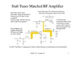
The questions below are in regards to an amplifier design shown below in the image and on slide 3 on the website: https://www.slideserve.com/liam/stub-tuner-matched-rf-amplifiers
Why does the input of the amplifier have the stub feeding into the bias resistor network, I thought its suppose to go to ground? My guess would be that its convenient, since it would take up less space and will obey the superposition principle?
Why couldn't have they used DC blocking capacitors before the transmission lines instead of after, couldn't that have kept them from having to use a bypass capacitor at the stub of the output?
How would you tell if this is a PA or and LNA?
