Continue to Site

Welcome to EDAboard.com

Welcome to our site! EDAboard.com is an international Electronics Discussion Forum focused on EDA software, circuits, schematics, books, theory, papers, asic, pld, 8051, DSP, Network, RF, Analog Design, PCB, Service Manuals... and a whole lot more! To participate you need to register. Registration is free. Click here to register now.

what is the number of fingers in MOS transistor

Status
Not open for further replies.

canarybird33

Member level 1
Joined
Apr 16, 2013
Messages
41
Helped
2
Reputation
4
Reaction score
2
Trophy points
1,288
Location
Mashhad, Iran, Iran
Activity points
1,591
Hello
I don't understand what it means?
"number of fingers"

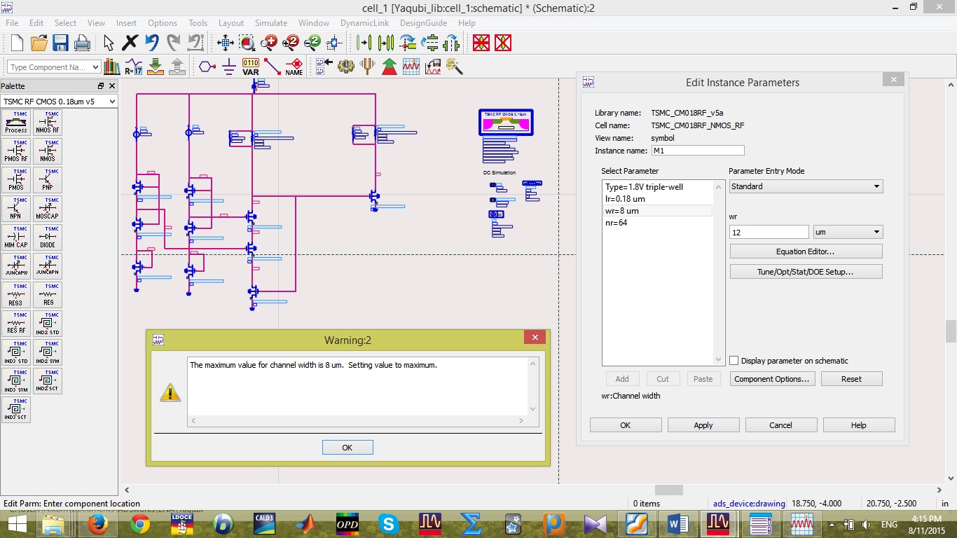
I am using TSMC180nm LIB in ADS, I wonder why the width of the transistor can't defined upper than 8 !!!

also number of fingers can not be more than 64.
why?
what am I suppose to do?


You cannot define the periphery/area of a MOS transistor as you wish. There are some technological constraints by foundry.
It has to be used as defined in foundry's design guides.
 
They are usually confidential, so you probably can't find them online easily. Even if you do you and the ones that are sharing it are infringing the agreement.

So the issue is that polysilicon is not a very good conductor and we usually try to avoid making huge gates. So instead of creating a milimeter long gate we usually divide it into sub units called fingers. And these fingers can be placed in a way to reduce the total area and parasitics. This placement is making them share drain or source with the next piece of gate.

Width can't be larger because the fab can't guarantee that the MOSs with your parameters would work up to spec. So they don't allow it but you can do it, they just wouldn't take responsibility. There should be a hard constraint switch in TSMC models, if you uncheck that it should allow.

Number of fingers is technically unlimited, but again that might be another rule I'm not aware of.

For quick reference, diffusion areas at the edges are 0.48 um long and width of the transistor wide. Diffusion areas for shared source/drains are 0.54 um long and width of the transistor wide. But it should calculate these values itself. I don't know why it's not doing it.

I don't know what you are supposed to do.
 
Status
Not open for further replies.

Part and Inventory Search

Welcome to EDABoard.com

Sponsor

Back
Top