narayani
Full Member level 2
Sir,
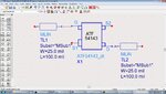
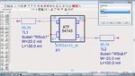
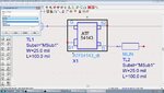
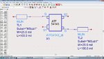
I want to generate the layout for ATF54143 transistor along with two MLIN's using Advanced design System 2011.10(ADS2011.10).
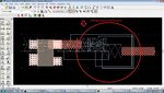
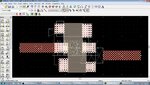
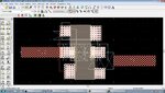
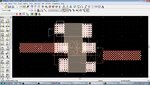
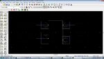
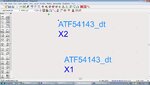
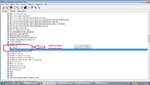
Now I generated the layout for ATF54143 transistor along with two MLIN's , have got layout generation, but it is not matching the schematic with ATF54143 and two MLIN,s. When I tried to generate the ATF54143 with two MLIN's, twice same ATF54143 transistor layout is generating in the layout view.
My question is, how to generate the proper layout generation for ATF54143 transistor and two MLIN's and also how to avoid the twice generation of same transistor layout in the layout view.
Related screen shots are attached.
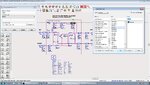
I want to generate the layout for ATF54143 transistor along with two MLIN's using Advanced design System 2011.10(ADS2011.10).
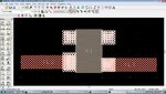
Now I generated the layout for ATF54143 transistor along with two MLIN's , have got layout generation, but it is not matching the schematic with ATF54143 and two MLIN,s. When I tried to generate the ATF54143 with two MLIN's, twice same ATF54143 transistor layout is generating in the layout view.
My question is, how to generate the proper layout generation for ATF54143 transistor and two MLIN's and also how to avoid the twice generation of same transistor layout in the layout view.
Related screen shots are attached.