Continue to Site

Welcome to EDAboard.com

Welcome to our site! EDAboard.com is an international Electronics Discussion Forum focused on EDA software, circuits, schematics, books, theory, papers, asic, pld, 8051, DSP, Network, RF, Analog Design, PCB, Service Manuals... and a whole lot more! To participate you need to register. Registration is free. Click here to register now.

How to eleminate floating point existence in AC-Coupled digital circuit

Status
Not open for further replies.

kooheyakhi

Newbie level 4
Joined
Jul 8, 2014
Messages
5
Helped
0
Reputation
0
Reaction score
0
Trophy points
1
Activity points
67
Hello there,
I have designed a 3-input NAND gate by capacitor network connected to a NOT gate.
this circuit functions well. recently i have found out that when inputs are stable and a noise occurs in node g, functionality of my circuit fails. this is because of node g which is floating point of my circuit. given that inputs are logical "111" and supply voltage is 0.65v. in this case, voltage level of node g is 0.65v (can be proved by super position).
now if a spike or noise ocurs and leads to pull node g to ground, then this node never comes back to Vdd and will stay at 0v.
is there any one help me?? the structure of circuit is in the following
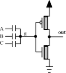
 

You want a pullup or pulldown resistor to take every input to
a known state absent any AC stimulus.

There is no picture although you appear to refer to one.
 
Fig 2.png

please help me. I think I should add some transistors to solve this problem, but I don't know how do it.
 

You ay that the node can be proven to assume the VDD
potential but I would like to see you manage that. If the
caps and gate dielectrics are ideal then you have no idea
what the gate potential will be (and your observations
bear this out).

Begin with just what you want this circuit to accomplish.
It looks like a capacitive summer, squared up. But that is
not an especially useful function, other than perhaps as
an exercise. Perhaps you want a linearizing feedback
resistor to auto-center the input to maximum sensitivity;
perhaps you want a pulldown to maximize noise margin
instead. Without knowing the purpose, you can't select
a plan.

Determinism is generally desirable. Work back from what
you want, to what makes it so, and I think circuit options
will suggest themselves as you go.
 

Hi,

I dont understand the function, but analog input to digital gate may cause problems.
Can you add pullup/pulldown on each input and feed each input to a schmitt trigger gate.
Then you get three clean digital signals.
Or use voltage comparators...

Klaus
 

I was aiming at realize a 3-input NAND gate with minimum number of transistors. if we implement it using CMOS logic we will need 9 transistors. but in my circuit there is just 2 transistors. this idea leads to decrease the total number of transistors and power consumption.

there is four possible cases in the inputs. (given supply voltage is .9v)
case1: all inputs are logical '0' then node g is 0v.
case2: one of inputs are logical '1', then node g is 0.3v.
case3: two of inputs are logical '1', then node g will be 0.6v.
case4: all inputs are logical '1' then node g will be 0.9v.

so far we have designed a voltage divider which produces 4 level of voltages. now if we set a proper threshold voltage for NOT gate such that it switches to ground when the voltage of node g is greater than 0.6v (note that this ocure only in case4, i.e., all inputs are logical '1' ), in fact we have implemented a NAND function. in cases 1, 2, and 3 which voltage of node g is less than 0.6v, NOT gate will not switch and its output remains at 0.9v or logical '1'.

I could implement voltage divider using resistors, instead capacitors. If I did this then there would be a large static power consumption. given one of inputs are '1' and other are '0'. therefore there is a path between resistors that consumes power. in conclusion I chose capacitor network. when it fully charges then there will not be any path.

this structure functions well, without problem. but recently i found that when inputs are stable for example at logical "111" and now if a noise cause to pull down the voltage of node g from 0.9v to 0v, it will never restores to 0.9v. because we know that in DC state capacitors are open circuit. (in other words, node g is floating point)

Now I am looking to solve this problem. there are some solutions:
1- design a new voltage divider using MOSFETs. because implementing resistors in VLSI is hard.
2- There should be a DC path to floating point to set its DC operating point, otherwise it is vulnerable to noise.

I hope that I could explain my goal
 

You do realize that any capacitor able to deliver useful charge
to the gate node, will be as large or larger than a FET (like,
if you wanted even 30% of voltage the individual caps would
be like 10X C, hence 10X gate area, plus whatever you lose
for the parasitic Cs and contact area).

Your "cases" all seem to have an assumed initial condition of
"node g", but this is an assertion and not a consistent reality.
Your intermediate cases with 0.3 and 0.6V still give you high
static current.

This is not really a NAND3 function; if the threshold is really
VDD/2 then what you have is a dynamic majority voter.

A 3-input NAND will have the NMOS stack only trivially larger
than a single stripe FET, if you draw it without contacts between
gate stripes. The PMOS will dominate area, and need full
contacting. I think an unbuffered gate will probably fit within
the contact-pitch-degined cell width, height being likely
determined by more complex gates (FFs probably), so the
optimization of this particular gate probably doesn't deserve
heroic effort.
 

Status
Not open for further replies.

Part and Inventory Search

Welcome to EDABoard.com

Sponsor

Back
Top