Continue to Site

Welcome to EDAboard.com

Welcome to our site! EDAboard.com is an international Electronics Discussion Forum focused on EDA software, circuits, schematics, books, theory, papers, asic, pld, 8051, DSP, Network, RF, Analog Design, PCB, Service Manuals... and a whole lot more! To participate you need to register. Registration is free. Click here to register now.

Implicitly connected AGND still shows up as airwires to be routed (EAGLE)

Status
Not open for further replies.

randomshinichi

Newbie level 6
Joined
Jul 23, 2013
Messages
13
Helped
0
Reputation
0
Reaction score
0
Trophy points
1
Activity points
164
agnd.png
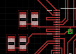
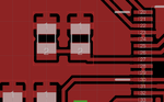
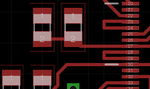
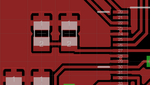
As you can see, EAGLE tells me that 24 needs to be connected to 28, which is connected to 29, which also connects to pin 31. Also, 10 needs to be connected to 8. (These are all ground)

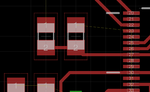
The problem is, I already made vias between the ground planes on both sides of the board, but the airwires still show up (and you can see that there are no "islands" in the blue ground plane either). In other parts of the board EAGLE is smart enough to see that I have a via and the airwire disappears, but in this case they remain. Am I doing something wrong, or is EAGLE doing something wrong?

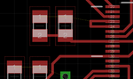
EDIT: FYI the green through-hole pin on the right marked "2" is the ground.
 

Here's some thoughts :

Try removing your forced vias, and see what Eagle does.
Make sure your routing grid is small enough for the IC pads spacing.
Check other layers in case you are missing something which is invisible here.
 

Also, do a 'ratsnest' and ensure that the option that the "ratsnest processes polygons" option is ON. Do a DRC.

Keith
 
Last edited:

I figured out what happened. Although it looks like they're connected in my opening post, the red of the IC's pins is actually not connected to the red of the ground plane (EAGLE sucks balls, someone really needs to come up with a better designed software package). I had to route a wire out to the ground plane explicitly, and then EAGLE considered the route part of the ground plane and accepted the connection.

Also, despite what it looks like in the first image in the opening post, I never connected the two adjacent pins explicitly. The ground plane was supposed to reach both of them. So I drew these loops instead to make the pins reach the ground plane and connect them to each other.

This would never have happened if EAGLE wasn't such a poorly written POS.
 

Attachments

  • Screen Shot 2013-10-01 at 4.52.33 PM.png
    Screen Shot 2013-10-01 at 4.52.33 PM.png
    38.5 KB · Views: 84

I figured out what happened. Although it looks like they're connected in my opening post, the red of the IC's pins is actually not connected to the red of the ground plane (EAGLE sucks balls, someone really needs to come up with a better designed software package). I had to route a wire out to the ground plane explicitly, and then EAGLE considered the route part of the ground plane and accepted the connection.

Also, despite what it looks like in the first image in the opening post, I never connected the two adjacent pins explicitly. The ground plane was supposed to reach both of them. So I drew these loops instead to make the pins reach the ground plane and connect them to each other.

This would never have happened if EAGLE wasn't such a poorly written POS.

A bad workman blames his tools. I have been using Eagle for a long time and never had the problem you describe. You need to learn how to use the tools rather than complaining about them. I don't know how you got your layout into such a muddle but a logical workflow and regular DRC while you are laying out a board would probably help.

Keith
 

A bad workman blames his tools.

I agree. It would be interesting to learn how the OP actually figured out the source of his problem so quickly, after reading the responses here.
Like all complex and evolving software, EAGLE has its intricacies, and it's not the first which has required a guru to point out the obvious.
 

I figured it out when I ripped up a signal that was blocking and routed from one pin to the other just because I was frustrated - that's when I noticed that the airwire changed direction and disappeared.

There are two kinds of tools: one that requires that the user adapt to it, and one that simply fits in the hand like it was made for it. Having trouble finding that last airwire to route; cryptic DRC errors that never say what's really wrong (would it kill someone to say Drill Size larger than allowed value instead of just saying Drill Size?); the way renaming a device in the library works; you can hide airwires of a specific net with a click but to unhide them you have to type a command... and now misleading crap like this. A tool, properly designed, should get out of the way, not get in the way and force you to learn its "intricacies".
 

You really need to learn your tools instead of blaming them for your inexperience with electronics design and PCB layout, as with your earlier post https://www.edaboard.com/threads/296356/ If you try some other design tools you will find the issues you are having are not unique - they come under the category of "user error". I do hope you are not serious that a "drill size" error was too cryptic and you had problems deciding if the error was that it was too large or too small!

I also don't understand how you "fixed" the problem. You now seem to have no ground plane. Also, you do not have to join pads with a track which are going to be connected with a ground plane flooded over them - Eagle will make the connection to a valid, correctly named polygon and add thermals as required. Your ground pins are now joined to the adjacent pins but not to a ground and yet there are no airwires. Your "solution" doesn't make sense.

Keith
 

You really need to learn your tools instead of blaming them for your inexperience with electronics design and PCB layout, as with your earlier post https://www.edaboard.com/threads/296356/ If you try some other design tools you will find the issues you are having are not unique - they come under the category of "user error". I do hope you are not serious that a "drill size" error was too cryptic and you had problems deciding if the error was that it was too large or too small!
I admit my inexperience with this sort of work. But this is exactly why I am in a good position to comment, because I am not "used" to any particular program. Once you have adapted your mind to a particular software package, it's no wonder you think it's perfectly adequate for everything.

I also don't understand how you "fixed" the problem. You now seem to have no ground plane. Also, you do not have to join pads with a track which are going to be connected with a ground plane flooded over them - Eagle will make the connection to a valid, correctly named polygon and add thermals as required. Your ground pins are now joined to the adjacent pins but not to a ground and yet there are no airwires. Your "solution" doesn't make sense.

Keith
OK, let's start with 0.png. The airwires are there.
0poly.png: After running rats, these pins still aren't connected, even though the red filling clearly touches the pins and is connected. The airwire shows.

1.png:Now I run ripup @; and place a loop.
1poly.png:Now one airwire is definitely gone - but 29 and 31 also need to be connected. So I place another loop:

2.png
2poly.png: and finally, the airwires are gone, presumably because they were never connected through the ground plane in the first place.
 

Attachments

  • 0.png
    0.png
    37.5 KB · Views: 82
  • 0poly.png
    0poly.png
    40.7 KB · Views: 80
  • 1.png
    1.png
    42.3 KB · Views: 97
  • 1poly.png
    1poly.png
    39.4 KB · Views: 84
  • 2.png
    2.png
    35.1 KB · Views: 87
  • 2poly.png
    2poly.png
    43.4 KB · Views: 84

The settings for your polygon make it impossible to reach the pads of the IC - the thermal spokes are too large. Hence the reason why it connects when you pull out a loop of copper. You need to set the "width" of track used to make the polygon to a size suitable for connecting to the IC pads, then it will connect without the loop. Generally, the pad width is a good choice, or slightly smaller. If you want large thermals for some components and smaller for others, simply use two polygons with different track widths and overlap them.

I would probably have spotted it sooner but the image in your first post shows the ground over the IC pins but with airwires still there. None of your later posts show that. It is always easier to post the board files to find problems like this rather than just images.

Keith
 

There are two kinds of tools: one that requires that the user adapt to it, and one that simply fits in the hand like it was made for it. Having trouble finding that last airwire to route; cryptic DRC errors that never say what's really wrong (would it kill someone to say Drill Size larger than allowed value instead of just saying Drill Size?); the way renaming a device in the library works; you can hide airwires of a specific net with a click but to unhide them you have to type a command... and now misleading crap like this. A tool, properly designed, should get out of the way, not get in the way and force you to learn its "intricacies".
I wish after 28 years of doing PCB design and still learning how to do things in the package I use I could have your arrogance, though this seems to be the way it is theses days, instant experts. I would suggest you put some effort into learning the software, rather than decrying it. it takes a lot of learning, both of software, electronics, physics, EMC SIV etc to be a top flight PCB designer theses days, there are no easy routes other than applying yourself.
 
The settings for your polygon make it impossible to reach the pads of the IC - the thermal spokes are too large. Hence the reason why it connects when you pull out a loop of copper. You need to set the "width" of track used to make the polygon to a size suitable for connecting to the IC pads, then it will connect without the loop. Generally, the pad width is a good choice, or slightly smaller. If you want large thermals for some components and smaller for others, simply use two polygons with different track widths and overlap them.

I would probably have spotted it sooner but the image in your first post shows the ground over the IC pins but with airwires still there. None of your later posts show that. It is always easier to post the board files to find problems like this rather than just images.

Keith
That solved the problem, thanks! I set it to 0.008, hopefully that'll be enough for the currents.

I wish after 28 years of doing PCB design and still learning how to do things in the package I use I could have your arrogance, though this seems to be the way it is theses days, instant experts. I would suggest you put some effort into learning the software, rather than decrying it. it takes a lot of learning, both of software, electronics, physics, EMC SIV etc to be a top flight PCB designer theses days, there are no easy routes other than applying yourself.
Nobody's saying that being a PCB designer is easy. Then again, nobody's saying it should take 28 years to learn how to use a software package either. It's a tool. Learning how to use the tool is not the achievement. Making something with it is.
 

PCB design has changed a lot over the last 28 years and the package I have used has changed accordingly, so it is a continual learning process. I started out doing manual tape ups with red and blue, early CAD systems were not like todays, initial schematic capture programs were horrendous, hence the popularity of Orcad, because they were one of the first to make them a more useful tool.
Learning how to use the tool is not the achievement.
That is a comment that someone who will never master a tool, if you don't master the tools you use, the only thing you will produce is mediocre rubbish. Learning to use the tools of your trade is paramount in any profession you choose.
 
Status
Not open for further replies.

Part and Inventory Search

Welcome to EDABoard.com

Sponsor

Back
Top