Continue to Site

Welcome to EDAboard.com

Welcome to our site! EDAboard.com is an international Electronics Discussion Forum focused on EDA software, circuits, schematics, books, theory, papers, asic, pld, 8051, DSP, Network, RF, Analog Design, PCB, Service Manuals... and a whole lot more! To participate you need to register. Registration is free. Click here to register now.

Multiple VDD -- transition from one VDD to another.

Status
Not open for further replies.

lambchops511

Member level 1
Joined
Oct 10, 2011
Messages
38
Helped
0
Reputation
0
Reaction score
0
Trophy points
1,286
Activity points
1,539
I am using CMOS IBM 180nm (High Voltage Option)

I have two parts of the circuit... A and B

A is VDD 1.8
B is VDD 5

A drives logic which will signal something to be B to do something...


How would I implement this?

How do I transition from VDD 1.8 to VDD 5?

Can I just change the body connection of the B to use VDD1.8 bias instead of VDD5 ? would that work?

Thanks.

---------- Post added at 00:14 ---------- Previous post was at 00:12 ----------

Or do I need to use something like an amp to amplify my signal from VDD1.8 to VDD5 ... thanks.


thank you. I guess there is no more efficient to do it... Because I have many of these signals that need to be converted. Thanks.
 

Typically a transistor is used to shift voltage level upward.

To shift downward a resistor divider may be okay. But only if it doesn't ruin impedance matching.

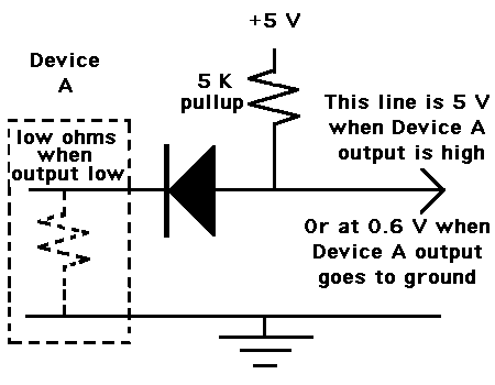
Here's a simple scheme that may work on the condition that your Device A connects the output to ground internally when output goes low. (In other words the output must sink current.)

Furthermore your next stage must recognize 0.6 V as a low.

31_1325041316.gif
 

the schematic you drew... i don't think it will work if i go from 1.8V to say 15V VDD correct? I am actually using 15V VDD in my second circuit (using IBM 180 HV allows up to 50 V). Thanks.
 

the schematic you drew... i don't think it will work if i go from 1.8V to say 15V VDD correct? I am actually using 15V VDD in my second circuit (using IBM 180 HV allows up to 50 V). Thanks.

The same schematic will work but you must pay attention to component values so as to prevent an overload. It's a dirt simple method and it depends on other things being right for it to work.

The diode prevents interaction between your 1.8V device and the following stage. The only possible interaction is for current to flow down to ground through an existing internal pathway in your 1.8V device (that is, if there is a low impedance internal pathway). Come to think of it, there ought to be a resistor inline with the diode just in case your next stage were to send overmuch current flow back into your 1.8V device.

You mention 50V. If that is present then the diode should have a higher reverse V rating to suit.

The pullup resistor is a typical method that works in many cases. It is also incorporated when using a transistor for level shifting.

For your purposes you may wind up needing a transistor-based level shifter.
 

I'm trying to use:

**broken link removed**


however its not working and I cant seem to find out the problem... for the "Level Translating Block" ... the Body Connections for the PMOS -- should they connect to the Vccb as well right?

---------- Post added at 09:10 ---------- Previous post was at 09:08 ----------

ah- nvm . i got it working . stupid typo. thanks all!
 

Status
Not open for further replies.

Part and Inventory Search

Welcome to EDABoard.com

Sponsor

Back
Top