deniah
Member level 4
- Joined
- Nov 28, 2005
- Messages
- 74
- Helped
- 6
- Reputation
- 12
- Reaction score
- 5
- Trophy points
- 1,288
- Location
- Montenegro
- Activity points
- 1,777
Hello
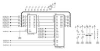
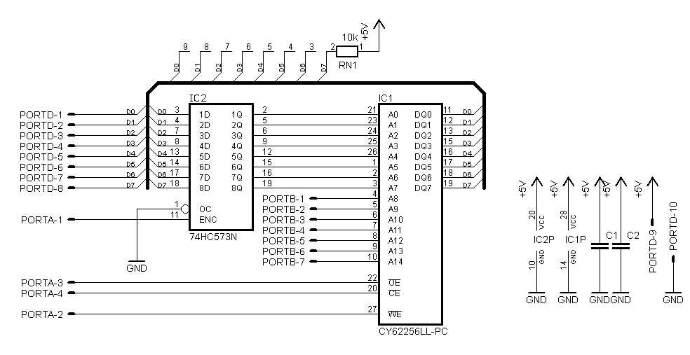
I'm trying to access SRAM 62256 but all I get is 0xFF or some random data. SRAM is connected as in the schematic. MCU is a PIC18F452, xtal 8MHz (HS).
Here is code for reading and writing:
From 62256 datasheet:
for /CE:
/CE is active LOW. Chip enable must be active when data read form or write to the
device. If chip enable is not active, the device is deselected and is in standby power
mode. The DQ pins will be in the high impedance state when the device is deselected.
for /WE:
The write enable input is active LOW and controls read and write operations. With the
chip selected, when /WE is HIGH and /OE is LOW, output data will be present on the
DQ pins; when /WE is LOW, the data present on the DQ pins will be written into the
selected memory location.
and for /OE:
The output enable input is active LOW. If the output enable is active while the chip is
selected and the write enable is inactive, data will be present on the DQ pins and they
will be enabled. The DQ pins will be in the high impendence state when OE is inactive.
Can someone tell me where I am getting wrong.
---------- Post added at 16:48 ---------- Previous post was at 16:33 ----------
I just realized that my eagle library was mixed up. Component marked as 74HC573 was actually 74HC373.
I'm trying to access SRAM 62256 but all I get is 0xFF or some random data. SRAM is connected as in the schematic. MCU is a PIC18F452, xtal 8MHz (HS).
Here is code for reading and writing:
Code:
#define HC573_LE LATA.F0

#define RAM_WE   LATA.F1
#define RAM_OE   LATA.F2
#define RAM_CE   LATA.F3

void init() {
   ADCON0 = 0;
   ADCON1 = 7;

   TRISA = 0;
   TRISB = 0;
   TRISC = 0;
   TRISD = 0;
   TRISE = 0;

   LATA = 0;
   LATB = 0;
   LATC = 0;
   LATD = 0;
   LATE = 0;

   UART1_Init(9600);
   Delay_ms(100);

   HC573_LE = 0;
   RAM_OE = 1;
}

void Write_62256(unsigned int address, char _data) {

   TRISD = 0b00000000;

   HC573_LE = 1;
   LATD = ((char *)&address)[0];  //  LATD = lo(address);
   HC573_LE = 0;

   LATB = ((char *)&address)[1];  //  LATB = hi(address);

   RAM_CE = 0;	// chip select is active lo
   RAM_WE = 0;	// write enable is active lo
   RAM_OE = 0;	// output enable is active lo

   LATD = _data;

   RAM_WE = 1;
   RAM_OE = 1;
   RAM_CE = 1;
}

char Read_62256(unsigned int address){

   char data_read;

   TRISD = 0b11111111;

   HC573_LE = 1;
   LATD = ((char *)&address)[0];  //  LATD = lo(address);
   HC573_LE = 0;

   LATB = ((char *)&address)[1];  //  LATB = hi(address);

   RAM_CE = 0;
   RAM_WE = 1;
   RAM_OE = 0;

   data_read = PORTD;

   RAM_OE = 1;
   RAM_CE = 1;

   return(data_read);
}

void main() {
   init();

   write_62256( 0x0100, 128 );
   write_62256( 0x0200, 127 );

   while(1) {
      UART1_Write(read_62256(0x0100));
      Delay_ms(500);
      UART1_Write(read_62256(0x0200));
      Delay_ms(500);
   }
}
From 62256 datasheet:
for /CE:
/CE is active LOW. Chip enable must be active when data read form or write to the
device. If chip enable is not active, the device is deselected and is in standby power
mode. The DQ pins will be in the high impedance state when the device is deselected.
for /WE:
The write enable input is active LOW and controls read and write operations. With the
chip selected, when /WE is HIGH and /OE is LOW, output data will be present on the
DQ pins; when /WE is LOW, the data present on the DQ pins will be written into the
selected memory location.
and for /OE:
The output enable input is active LOW. If the output enable is active while the chip is
selected and the write enable is inactive, data will be present on the DQ pins and they
will be enabled. The DQ pins will be in the high impendence state when OE is inactive.
Can someone tell me where I am getting wrong.
---------- Post added at 16:48 ---------- Previous post was at 16:33 ----------
I just realized that my eagle library was mixed up. Component marked as 74HC573 was actually 74HC373.