dgnani
Advanced Member level 1
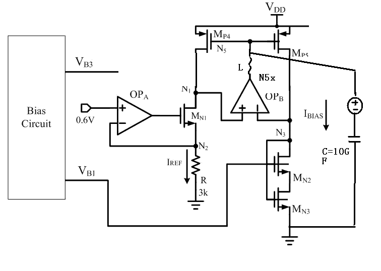
not sure what simulator are you using? if spectre useI didn't understand this and I think that's the reason I'm having a difficulty on plotting the data. I did include these codes the .print vdb(n5) vdb(n3). AOL(dB) = N5(dB) - N3(dB). Is this correct? I inserted the "vn1 vn1 gnd dc 0V ac 1V" at the positive input of the OP.
dB20(V(VN5) / (V(N1)-V(N3)))
phase(V(N5) / (V(N1)-V(N3)))
for eldo just plot
V(N5) / (V(N1)-V(N3))
it will give both magnitude in dB and phase automatically
your source has to break the wire not drive it, it should be something like
vn1 n1 n1_old dc 0V ac 1V
where you rename all other previous n1 nodes as n1_old except for the opamp input which is still n1
But right now it does not matter (at least not to solve your problem)...
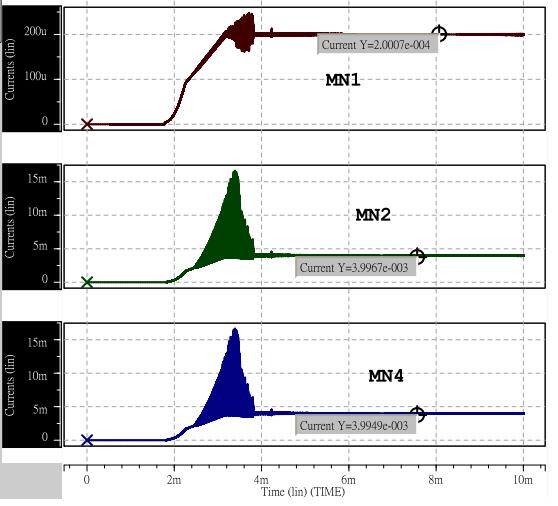
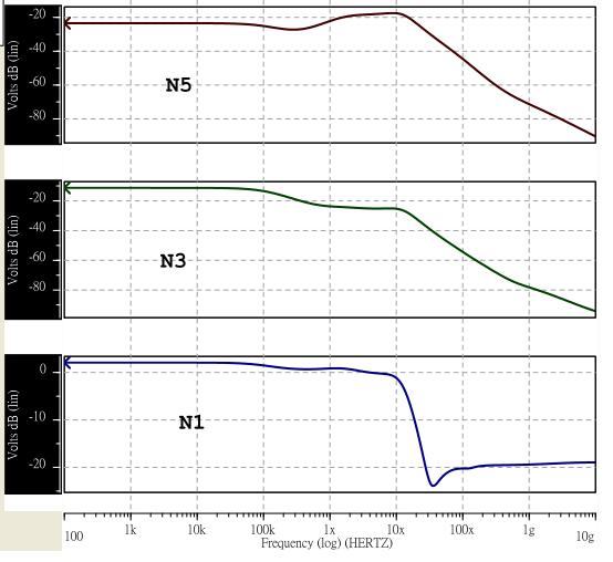
... I finally noticed that your N1 and N3 do track nicely so gain was there, I misunderstood post #8 where you described N1 and N3 behavior I thought they were at different voltages
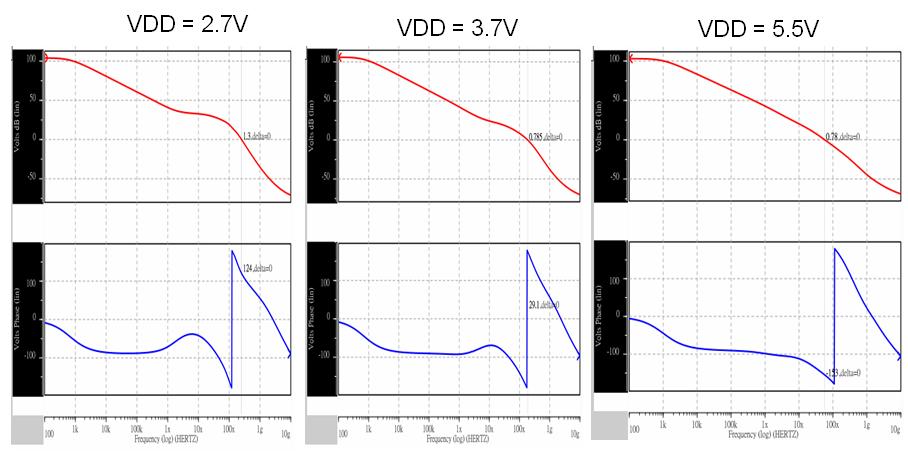
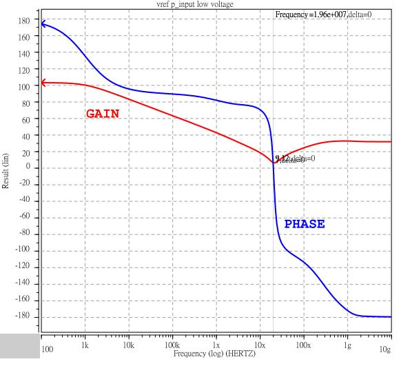
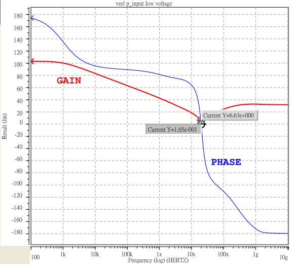
Congratulation Leo_o2, the new plots show clearly a second OP, now it is just a question of stabilizing the loops, a good cap in the right place will probably do the trick...
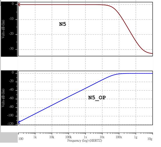
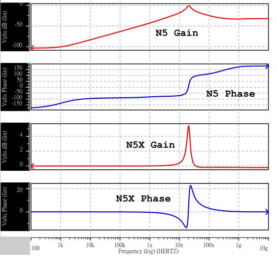
I guess allennlowaton you can try that next to see how your loop gain looks in the circuit, just break the output wire instead of the input one and look at
L=v(n5_opamp)/v(n5)
after inserting
vn5 n5 n5_opamp dc 0V ac 1V
and connecting the opamp output to n5_opamp instead of n5
do this at the OP where you see the oscillation
The circuit apparently still works but you'll like it better w/o the ringing, I'm sure
Last edited: