G0HZU
Full Member level 3
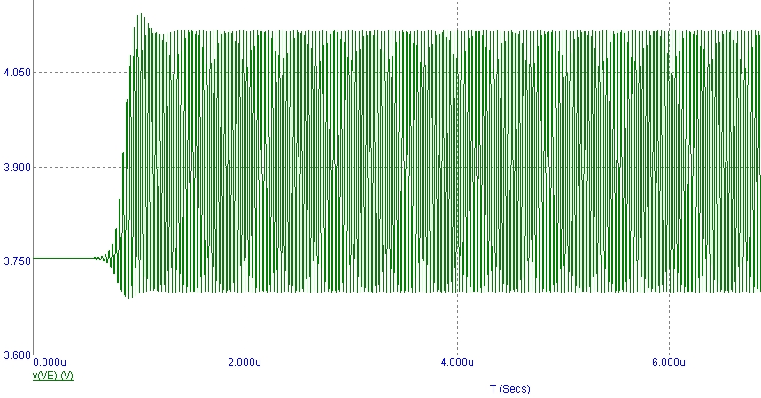
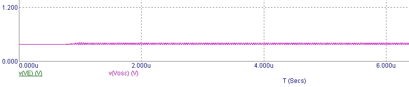
Even if the OP put the highest quality 430nH inductor in the World in this circuit it would be severley damped by the 1k collector resistor that is effectively in parallel with it.
The oscillator is still an epic fail despite all the posts offered to the OP.
I gave a revised circuit that would oscillate in an earlier post but maybe the goal is to try and make the original circuit oscillate despite it being 'wrong' for so many reasons...
The oscillator is still an epic fail despite all the posts offered to the OP.
I gave a revised circuit that would oscillate in an earlier post but maybe the goal is to try and make the original circuit oscillate despite it being 'wrong' for so many reasons...
")