Continue to Site

Welcome to EDAboard.com

Welcome to our site! EDAboard.com is an international Electronics Discussion Forum focused on EDA software, circuits, schematics, books, theory, papers, asic, pld, 8051, DSP, Network, RF, Analog Design, PCB, Service Manuals... and a whole lot more! To participate you need to register. Registration is free. Click here to register now.

PD20015E _Imedance_matching issue at 2GHZ

Status
Not open for further replies.

adnan012

Advanced Member level 1
Joined
Oct 6, 2006
Messages
468
Helped
2
Reputation
4
Reaction score
2
Trophy points
1,298
Activity points
4,923
hi,

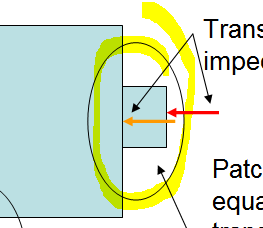
At page 6 of the data sheet Zin and ZDL is mentioned with arrows.

AT 2 G Hz

Zin is 0.45 + J0.99
ZDL is 0.99 - J0.90

I am confused when i compare these values to the obtained from ADS simulation. What is the meaning of Zin and ZDL in case of matching to 50 OHM.

Should I match Zin or conjugate of Zin to 50 0hm?
Should I match ZDl or conjugate of ZDL to 50 0hm?
 

Attachments

  • PD20015-E.pdf
    350.4 KB · Views: 75

Conj{Zin} should be matched to 50 Ohm..
But ZDL is the Load Impedance that is also Conj{Zout}.
However, if this component will be used as a high power device, this won't probably valid anymore.In this case Optimum Load Impedance should be
found for specific application and frequency.
 
Thanks a lot.
At the first page read the lines which are high lighted. What does it mean. Can i use the device at 1800MHz. Is it a 1 GHz device or 2GHz device? I have tested it up to 1100MHZ but after that it shows now gain at all.
 
Last edited:

Thanks a lot.
At the first page read the lines which are high lighted. What does it mean. Can i use the device at 1800MHz. Is it a 1 GHz device or 2GHz device? I have tested it up to 1100MHZ but after that it shows now gain at all.

There is discrepency between the phrases but second phrase is not consistent.If you look at the specifications, you'll see that the transistor can operate upto 2GHz.
I believe it can be used upto 2GHz with 13.6VDC supply voltage giving 15W Output Power@2GHz.But the supplied data is very poor to design such an amplifier.
You'll need more and more data and model...
Because the frequency is pretty high
..
 
i have ads model for the device.

I followed the following design procedure.

1) Performed Small signal s-parameters simulation plus DC analysis.
2) ADS Load PULL test.
3) Picked appropriate Load impedance plus input and Transformed/matched it to 50 ohm.
4) Used ADS Momentum analysis to design transmission line matching network with bias network.

My pcb is double sided FR4 1.6mm with 1 oz copper. All tracks and micro strip lines have "soldering mask" on it.

My testing procedure is that, first Set proper VDD and Idq and then connect the amplifier
with VNA (in Forward Transmission test mode) with a 20 db 10 watt attenuator in series with
amplifier output port (VNA RECEIVER PORT). I get -20db (0 db with out attenuator) gain in the desired frequency range (1800-1830MHz) . When Idq is increased by increasing the Vgs i get -17dbm to -15dbm (3 to 5 db gain without attenuator) but the device become too hot.
Sometimes, while tuning the input and out put matching networks with the SMD trimer (included in the matching network design), the amplifier shows 15 db gain ONLY at a very particular frequency. Sometimes amplifier begins to oscillate at different frequencies during tuning.

Before this, have successfully designed 900MHz, 10-15 watt amplifier with the same LDMOS by following the same procedure
 

What is the method of mounting ldmos leads (BLL1214-250R) (or any other device) to micro-strip type matching network. Should i include copper footprint for the ldmos input/output pin, in the ads simulation as shown in the file.
 

Attachments

  • LDmos mounting .ppt
    291 KB · Views: 71

Should i include copper footprint for the ldmos input/output pin

It is very important to have the correct line width at the transistor side, i.e. include the step in line width between the matching circuit and the transistor terminal width.
 

Thanks for reply.

Can you explain in detail with graphical example.
 

it means that, transistor lead will sit completely on the right most patch. ads simulation differs when i include that area.

---------- Post added at 18:30 ---------- Previous post was at 18:01 ----------

Suppose that transistor input lead is soldered to a micro strip line of the same size. now what will be the input impedance of the transistor. I think it will not remain same.
 

it means that, transistor lead will sit completely on the right most patch. ads simulation differs when i include that area.

Yes and yes.

It must be different, because that step in width makes a big difference. If you do not include that metal segment, the Momentum port will be very wide, over the complete width of the capacitive patch. That would be wrong. The port width should be the same as the component terminal width.

With the port attached to the small metal patch, you force the current to exit at the correct place with the correct terminal width.
My clients who design power amplifier layout with Sonnet EM set the port width of the transistor component in Sonnet. In Momentum, the work around is to have a metal with the correct width and connect the port there.


Thanks for reply.

How can i represent a capacitor in momentum .
Where should i connect port3 in momentum.

"In Momentum, the work around is to have a metal with the correct width and connect the port there."
 

Attachments

  • port placement in momentum .ppt
    315 KB · Views: 112

I don't know about your SMD capacitor. This was not needed in my designs. Are you sure that you want a component, and not include this capacitance in layout (bigger patch)?

But assuming that the SMD capacitor is correct, I would add a little rectangle that represents the capacitor pad width and place the port there. Connection must be done inside the ADS circuit similator, because you can not place components directly in Momentum. Take the ADS data block to the schematic and connect the cpacitor there.
 

I am not sure what the question is? Are you still unsure about this port?

93_1324023550.png


Looks good to me. Just make sure that the port reference plane is the same as in the transistor data. My guess is that the data is measured to the package (excluding leads), so that the lead/pad length should indeed be part of your EM model.

~~

The PDF that you linked has incorrect URL.
 

"I would add a little rectangle that represents the capacitor pad width and place the port there"

what value you will assign capacitor port?

---------- Post added at 09:29 ---------- Previous post was at 09:24 ----------

i want to know that in momentum there are two options to connect the transistor input port. one at the edge of the patch (red color) second at the point between transistor mounting patch and the rest of the matching network (orange coclor)

---------- Post added at 09:32 ---------- Previous post was at 09:29 ----------

https://www.wpi.edu/Pubs/E-project/...2408-050647/unrestricted/Konca_Miller_MQP.pdf
 

what value you will assign capacitor port?

It makes no difference, because the correct capacitor value must be connected in ADS schematic. Use default port impedance 50 ohm in Momentum, and then connect the correct capacitor value in ADS schematic.

i want to know that in momentum there are two options to connect the transistor input port. one at the edge of the patch (red color) second at the point between transistor mounting patch and the rest of the matching network (orange coclor)

RED, i.e. edge port at the polygon that represents the pads/leads.

---------- Post added at 10:06 ---------- Previous post was at 09:46 ----------

I look at the transistor data sheet again and see that the "leads" are very short. The length of the polygon representing the leads must be short then, of course.

29_1324026343.png
 

Do you have ADS 2011 . I want to share ads files.
 

Status
Not open for further replies.

Part and Inventory Search

Welcome to EDABoard.com

Sponsor

Back
Top