Continue to Site

Welcome to EDAboard.com

Welcome to our site! EDAboard.com is an international Electronics Discussion Forum focused on EDA software, circuits, schematics, books, theory, papers, asic, pld, 8051, DSP, Network, RF, Analog Design, PCB, Service Manuals... and a whole lot more! To participate you need to register. Registration is free. Click here to register now.

Solder Mask over Bare Copper (SMOBC) question

Status
Not open for further replies.

RedAlert

Member level 1
Joined
Oct 13, 2001
Messages
38
Helped
0
Reputation
0
Reaction score
0
Trophy points
1,286
Location
Somewhere in Israel
Activity points
176
Hi,

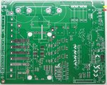
I do know what is SMOBC which is a polymer over the copper traces to protect them, prevent bridges in wave solder process and provide better look to the PCB board.
What I do not understand is that I see this solder mask layer applied to the rest of the PCB. if it is applied to the rest of the PCB then name SMOBC is deceiving a bit because the name implies it is for the copper traces only (Solder Mask over Bare Copper)

I've supplied a PCB image with two arrows (Red and Yellow) in the upper right. It is clearly seen that solder mask is applied to the trace as indicates the Red arrow, but near the Yellow arrow - is this a solder mask or a native color of the PCB material? also is it possible to spot the PCB Material from the picture (FR4?)?

I think that SMOBC used in the past only to the PCB traces but with time it is applied to the whole PCB. what do you think?

Thanks in advance.
 

Attachments

  • 3_3oz_Copper_PCB_Rigid_pcb.jpg
    3_3oz_Copper_PCB_Rigid_pcb.jpg
    275.6 KB · Views: 392

I have never seen it called solder mask "over bare copper" but solder mask has always covered the whole board with openings in the mask where soldering is required, as far back as I can remember.

Keith
 

Thanks for you feedback.

Actually there is SMOBC: **broken link removed** (I didn't create this value) and in lots referenes in google.
I think it is called historically SMOBC and probably in those days it covers only the bare copper but over time it is just called solder mask and cover the whole board except opening for pads when defined.

Someone knows how the solder mask layer is applied to the PCB ? especially how the process cover the opening from being solder masked ? for solder paste you use stencil but I guess that for solder mask you cannot use stencil, right?
 

I'm applying solder mask to the board, then put the board to the oven 100-120'C about 30 min. Then to the fridge about -17'C. Then to UV lamp with photo mask.
 
@keith1200rs

After more than 30 years in this field I will take your words for granted :)
PCB-POOL.COM link is really helpfull...

If I will summarize the general solder mask/resist process -
1) at start the soldermask process is applied to the whole PCB (even to the pads)
2) it is harden using UV with the circuit photo mask
3) after that it goes to the development where opening are made to the pads.

I got it right?
 

As I say, the name may be regional. I came across a term with PCBs recently which I had never heard but it was in common use in the USA.

I think the processing sounds right.

Keith.
 

I too have been in the PCB manufacture industry, when I was doing it we silkscreen printed the solder mask/solder resist whatever you wish to call it and yes it covers the entire board and always has.

It would not cover just the copper - it needs to also cover the laminate to make a seal between the copper and the laminate.

smobc is simply another term for it, even while covering the entire board it is still solder mask over bare copper.

Now it is applied differently but its still the same product.

Be it green, blue, red, white, black - it covers the whole board unless you put features in the solder mask where it is not to be covering the board.
 
Many years ago you got the solder mask applied over the tin/lead coating used for etch resist, this would re-flow causing bumps etc and was a problem with eurocards fitting in the card guides amongst other problems, then they decieded to put the solder mask over bare copper to combat this as this gentleman (below) puts more elegantly. Again I've always called it solder mask... This term is rather historical these days, the term and practice of putting solder mask over plated copper went out soon after SMD became more popular and HASL became the norm..


Quote.
HASL was a process to apply solder to the exposed copper on the boards, especially the pad areas and plated through holes. Prior to HASL, hot air leveling, there was a process called electroplated tin/lead which was used as an etch resist during the board fabrication process.

Once the board was etched the electroplated tin/lead coating was fused, or stated differently was reflowed. It was after this point in the process when the soldermask was applied to the board. This was the standard board process for plated through hole technology. When surface mount came about in the early 1980s and these boards were used, it was the first time that the entire board was subjected to the surface mount reflow processes of the time, which could have been anything from IR ovens, vapor phase systems, Convection ovens, etc..

It was also discovered that the solder expanded under molten conditions and the when the second side of the product was prepared for surface mount component assembly, solder balls were discovered all over the surfaces of the solder mask, especially over any of the conductor traces. It was at this time that the board fabrication process was changed to remove the tin/lead etch resist materials and leave the board simply as a copper board.

The soldermask was then applied over the bare copper, thereby eliminating the problems with solder balls migrating through the soldermask and interfering with the past deposition process on the second side of which was being assembled. After the soldermask was applied the board was then processed through a HOT Air Solder Leveling process coating all the exposed copper with solder, which became known as SMOBC, Soldermask over bard copper.

Leo Lambert, Vice President, Technical Director
EPTAC Corporation
leo@eptac.com
At EPTAC Corporation, Mr. Lambert oversees content of course offerings, IPC Certification programs and provides customers with expert consultation in electronics manufacturing
 
Status
Not open for further replies.

Part and Inventory Search

Welcome to EDABoard.com

Sponsor

Back
Top