Continue to Site

Welcome to EDAboard.com

Welcome to our site! EDAboard.com is an international Electronics Discussion Forum focused on EDA software, circuits, schematics, books, theory, papers, asic, pld, 8051, DSP, Network, RF, Analog Design, PCB, Service Manuals... and a whole lot more! To participate you need to register. Registration is free. Click here to register now.

RF PCB layout questions..beginners doubts.

Status
Not open for further replies.

themaccabee

Full Member level 4
Joined
Apr 1, 2007
Messages
201
Helped
6
Reputation
12
Reaction score
6
Trophy points
1,298
Activity points
3,003
Hi,

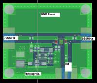
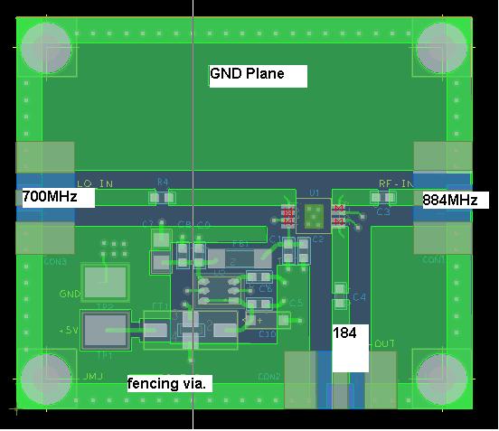
Im trying to do a layout for a mixer IC. HMC483..

Since im newbie ..i ve got a couple of questions..
The PCB is a two layer PCB.
Bottom layer is ground plane.
50Ohm impedance Tracks depending on PCB specs , has a width of 65mils..

My questions are..
1)Fencing Vias--Its Spacing & dia calculation.
2.)Is it necessary to provide guard vias for the 50Ohms impedance tracks along the ground plane adjacent to it..If needed how much spacing to be used?
3)Is there any spacing constraints to be maintained between 50Ohm impedance tracks and the adjacent ground planes on either side on the top layer?

Attaching the PCB view


Thanks & Regards
 

1. what is your freq? Normally vias is determined by PCB vendor, say 0.8mm/0.5mm
2. No. But place polygon for free PCB is a good habit.
3. You can calculate with TXLINE from AWR to calculate grounded coplar waveguide.
 
1. what is your freq? Normally vias is determined by PCB vendor, say 0.8mm/0.5mm

If you are mentioning the operating frequency..The RF freq =884MHz & LO=700MHz & IF=184 MHz..
Is that you meant?
Thanks &Regards
 

Some additional comments.
-I think you would want to use the minimal available via size in your technology to achieve best RF performance, e.g. 10-12 mils drill.
-If you take a look at the Hittite demo design, you'll realize, that they have a continuous top layer ground under the chip, connecting to top copper pour on both sides, also directly connecting all IC ground pins. That's much better than having individual GND vias with rather long (high inductance) traces as in your design.
-If you need "fence" vias at all, than near the transmission line, as shown in the Hittite layout example.
-You'll get some impedance discontinuities and parasitic via inductances by using a rather thick substrate. But I think it's no problem at < 1 Ghz.
- I agree that designing a grounded coplanar rather than pure microstrip is better in this case. The Hittite example also does in my understanding.
 
It will probably work. Make sure C1 is the smaller value than C2.

Also, you will have a little trouble soldering the chip to those three RF lines, because they are thermally massive compared to the other much smaller traces. The solder may not fully wet in the soldering time available. It is common to neck-down the RF traces so that just before they hit the device pins, they become smaller width.

And, as stated before, if there is going to be top layer ground metal, you need lots of via holes from it to the backside ground (I am assuming there is a backside ground plane?). IF you do not use a ton of vias, you can end up with an RF resonance.
 
Hi,

My questions are..
1)Fencing Vias--Its Spacing & dia calculation.
2.)Is it necessary to provide guard vias for the 50Ohms impedance tracks along the ground plane adjacent to it..If needed how much spacing to be used?
3)Is there any spacing constraints to be maintained between 50Ohm impedance tracks and the adjacent ground planes on either side on the top layer?
Thanks & Regards

1-Your frequency is very low so that the distance between fencing vias can be-for instance-1to 5mm
But you shouldn't neglect these vias where the ground connections are strictly needed , not only on borders..consider inside ground planes.Especially, decoupling capacitors need good ground connections and therefore you should put some extra vias close to these capacitors and consider again the vias for other components.
2and 3
If you get closer ground planes to track, the Transmission Line will become Grounded Co-Planar Waveguide instead Microstrip Line..
That's why, the width for 50 Ohm should be modified.I suggest you follow the app note..Keep-on the width and distance between TL and ground..
 
Hi,

Thank you all u guys for the replies..But im still partially clear about the subject..Forgive me my ignorance..

1-Your frequency is very low so that the distance between fencing vias can be-for instance-1to 5mm

When considering the fencing vias which frequency should i actually consider??RF/LO or IF?.Is it the highest frequency of all?
Also how could we say exactly the distance between fencing vias as 1-5mm

And, as stated before, if there is going to be top layer ground metal, you need lots of via holes from it to the backside ground (I am assuming there is a backside ground plane?). IF you do not use a ton of vias, you can end up with an RF resonance.
can some body explain me how this resonance occur?If im using the via how it is going away??


Ive seen a link
**broken link removed**
in which says
7) When you finish all the layers, fill the empty spaces with copper pour that is connected to the ground. Place vias that are connected to the ground layer with a distance of λ/20 cm between each other.
if it is true then how does the figure by 20 comes in??
 

you should consider the highest freq.
Your highest freq is 1G, so the wavelength in FR4 is about 300/sqrt(4)=150mm, so lamda/20=7.5mm.
For very high microwave, lamda/8 is OK.
Greater than lamda/4 is easily to resonate.
 
Status
Not open for further replies.

Part and Inventory Search

Welcome to EDABoard.com

Sponsor

Back
Top