Continue to Site

Welcome to EDAboard.com

Welcome to our site! EDAboard.com is an international Electronics Discussion Forum focused on EDA software, circuits, schematics, books, theory, papers, asic, pld, 8051, DSP, Network, RF, Analog Design, PCB, Service Manuals... and a whole lot more! To participate you need to register. Registration is free. Click here to register now.

[SOLVED] Problem with SMPS - No Output Volts

Status
Not open for further replies.

kkeeley

Member level 3
Joined
Jul 29, 2009
Messages
59
Helped
1
Reputation
2
Reaction score
1
Trophy points
1,288
Location
Australia
Activity points
2,890
Hi,

Sorry if this is a long post.

Overview:
I am working on a project where by I am rebuilding an existing working PC ATX power supply onto a new PCB so that the power supply can fit into the main unit of my overall project.
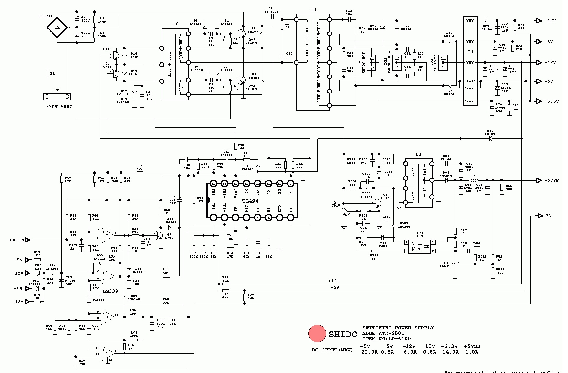
I have spent many days/weeks studying the existing circuit and drawing it in LTspice. I have also managed to find a schematic on the Web that is an exact match to the circuit I'm copying.

What I've Done so far:
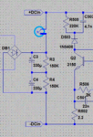
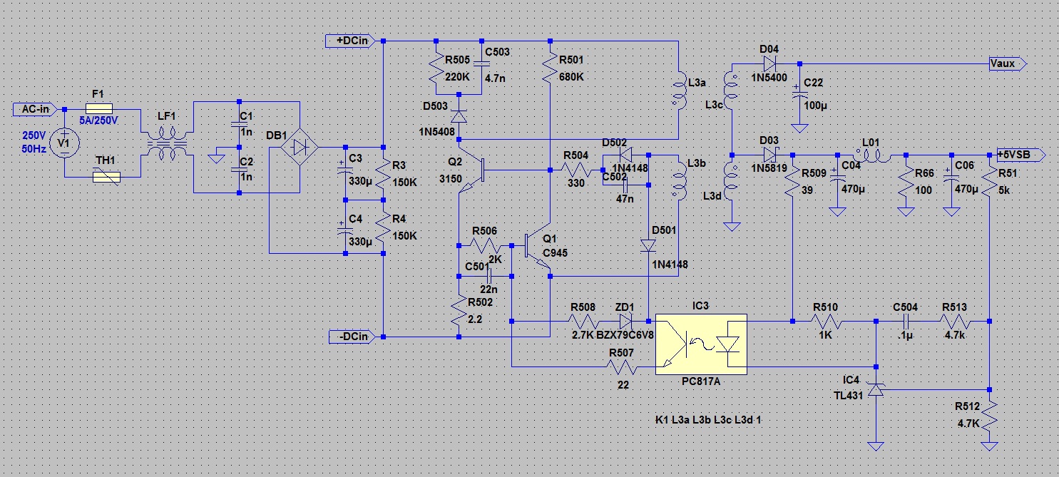
I decided that rather than building the entire circuit first I would just build the input recifiers and the +5V standby circuits. As seen in the attached image. LTspice shows this diagram to work and produce voltages. As I didn't wind the transformer myself I have had to guess/Play with the figures for the inductance of the inductors. I attached a red LED and 330R resistor to the +5V circuit and a 12V 50mA fan to the Aux circuit.


First attempt:
The first time I applied power to the circuit the led glowed and the fan ran (all was looking good), shortly after this both transistors and a few resistors self destructed in smoke. After removing all the visiblly damaged parts I found that the resistor I had use for R502 was an 18K instead of the 2R2. I replaced both Transistors and all resistors and caps on the high voltage side.

Current State of play:
After trying the circuit again the transistors went up in smoke again. At this point I replaced all parts on the high voltage side except for the transformer, which I didn't make as it is the one from the original circuit. Now the circuit no longer produces any output voltage and the fuse and other parts are not going up in smoke.

My Question:
As there are some rather high voltages involed in this circuit I would like to know firstly what might be the root cause of my problem? Are there any ways to lower the input voltage to a safer level and still have a working circuit? Can I test smaller parts of the circuit? Like checking that the transistors are oscilating as expected to product the AC voltage required on the transformer, etc.

Thanks for any help offered.
Kenneth
 

Did u check primary section diodes, IC3 and IC4?
 
Thank you for the suggestion,

I have already replaced IC3, but not yet replaced IC4, I will now replace IC4 as well and then re-test.

I will let you know the results.

Kenneth
 

I've been looking at the circuit you posted, and trying to find anything that doesn't look quite right there.
There's three areas which I think might be worth checking:
The midpoint between C3 & C4 looks as if it should be connected to something (perhaps just a 0v reference).
I can't see where the standing collector current into the output transistor of IC3 comes from (perhaps there's a wrong connection around D501 or ZD1).
The resistor values on the base of Q2 seem to lead to the wrong currents (perhaps wrong values or wrong connections?).

It would be worth applying a lower voltage to DCin & DCout for testing that Q1 & Q2 are switching correctly. If you can watch their collectors on a storage 'scope you can check the relative timing and perhaps a clue to the fault?

I would recommend checking everything in the switching part of your circuit against the original - I'm not confident that it is correct and you shouldn't put yourself in danger testing a suspect high voltage circuit!
 
Thanks for the reply,

The midpoint between C3 & C4 looks as if it should be connected to something (perhaps just a 0v reference).
This will be the 0V reference for the main transformer when added later.

I can't see where the standing collector current into the output transistor of IC3 comes from (perhaps there's a wrong connection around D501 or ZD1).
The resistor values on the base of Q2 seem to lead to the wrong currents (perhaps wrong values or wrong connections?).
The schematic I have drawn matches the schematic I found on the net for the SHIDO ATX 250 watt power supply which I have also attached.


It would be worth applying a lower voltage to DCin & DCout for testing that Q1 & Q2 are switching correctly. If you can watch their collectors on a storage 'scope you can check the relative timing and perhaps a clue to the fault?
Currently I don't have access to a storage scope, I only have an older 60Mhz analog scope.

Thanks for your ideas, I will keep checking over the circuit.
Kenneth

---------- Post added at 10:36 ---------- Previous post was at 09:51 ----------

Did u check primary section diodes, IC3 and IC4?
I have now replaced both IC3 and IC4 and I'm still getting the same results (No output volts)

I have also placed a 30v stepdown transformer between the 250v mains and my circuit. This gave me a consistent voltage of around 45v between the +/- DCin points. I don't have a larger 50Hz transformers to go higher with, and anything larger is rather expensive to buy around my area.

Thanks again,
Kenneth
 

Make sure you have the phasing of the L3a/b correct
 
Last edited:
PC power supplies seem to generally require a load on
either the +5V or +3.3V output, to defeat some open
circuit detect function. Which one, depends on the
generation of PC / supply. Try a 10 ohm resistor to
ground on each output in turn and see if any of them
do the trick. Then you can work on finding out if a
higher value will keep you lit and waste less power

I've cobbled a couple this way for 5V lab bricks.
 
Make sure you have the phasing of the L3a/b correct
As stated before, I did not make the transformer, it is the one from the orginal working power supply, The schematic works in LTspice, all be it that I have guessed the inductance values for each part of the transformer. So I don't think that this is the issue, also the circuit worked for a few seconds before smoking the transistors the first time it was powered up.

---------- Post added at 13:45 ---------- Previous post was at 13:41 ----------

Thanks for the suggestion.
PC power supplies seem to generally require a load on
either the +5V or +3.3V output, to defeat some open
circuit detect function. Which one, depends on the
generation of PC / supply. Try a 10 ohm resistor to
ground on each output in turn and see if any of them
do the trick. Then you can work on finding out if a
higher value will keep you lit and waste less power

I've cobbled a couple this way for 5V lab bricks.

I'll place a resistor on the 5V circuit to make it draw more power and see if this helps. 10 ohms should equal about 500mA so that's half the rated load.

Kenneth
 

I would concur with E-design. The transformer may be perfect but if either L3a or L3b connections are reversed it will not oscillate. Try reversing ONE of them and see what happens, don't reverse them both !!

Brian.
 

I agree with E-design and betwitxt that if one of the windings L3a or L3b was cross-wired (out of phase), then it is very unlikely to oscillate.
However, after staring at the circuits for some time, I'm still struggling to see how it could work (If there is a circuit error then it is in the original 'Shido' schematic as well as in yours).

I'm still not convinced the currents around the bases of the 2 switching transistors can be correct, which is, of course, critical. Referring to the brief period when your circuit powered a fan and an LED, I wonder if that energy could have been transferred during just one, initial, switch-on pulse, and that there was not a period of full oscillations?
I am also still unhappy with the lack of current source for the optoisolator; although this wouldn't stop it oscillating (it affects the feedback loop of voltage control), it does suggest that there is a possible error in the drawing.
Finally, your schematic shows D03 as a zenner, though this will not be the cause the problem either - just an observation.

If a simple reversal of either of the winding terminals still doesn't fix the circuit, I wonder if you might benefit from re-checking against the original PCB tracks around the bases of the 2 transistors Q1 and Q2 and the collector of the opto IC3?
Good luck!
 

It should be possible to check that the circuit is at least oscillating by lowering the 680k bias resistor to say 68k and test the circuit on a lower voltage lab supply (~30VDC) with current limit.
Then at least you can look at some waveforms without everything going up in smoke in a split second.

If you can't do that put a small wattage (around 5-10W) bulb rated at mains voltage in series with the DC supply to the switcher. The cold resistance of the bulb will allow the circuit to operate under very light loads while the hot resistance of the element will limit current to protect the circuit under fault conditions. Old trick used by TV repair guys to help fault find switching supplies.

Operation:
At the moment of applied DC initial turn on of Q2 is via R501 (680k). With Q2 turning on we get regenerative feedback via winding L3b. In other words as the dot end of L3a is pulled down through Q2, the non-dot end of L3b will move more positive providing more drive to Q2 base through D502, C502 and R504. This will cause Q2 to turn on quickly. Because of this current, the voltage over R502 will increase. When this voltage is enough (around 0.6 to 0.7V), Q1 will start to turn on and divert base current away from Q2. With base current being robbed from Q2, it will start to turn off. This will cause the collector voltage of Q2 to go up. Due to classic flyback action all winding voltages reverse and L3b will aid in turning off Q2 through C502 and R504 at this time. The maximum current flow is limited by R502 and turn on b-e voltage of Q1 (Imax = Vbe/R502). The feedback circuit through IC3 will help turn on Q1 and hence turn off Q2 sooner to establish voltage regulation action on the +5VSB line.
 

Attachments

  • protect.gif
    protect.gif
    55 KB · Views: 182
Last edited:
Thanks for your suggestions,
I agree with E-design and betwitxt that if one of the windings L3a or L3b was cross-wired (out of phase), then it is very unlikely to oscillate.
I will retrace the original PCB circuit and check If I have the transformer pins connected correctly.

Referring to the brief period when your circuit powered a fan and an LED, I wonder if that energy could have been transferred during just one, initial, switch-on pulse, and that there was not a period of full oscillations?
The fan and led both worked for about 20-30 seconds before the transistors went up in smoke that first time. Would this not have been longer than what the initial switch-on pulse could provide? If so then this may indicate that the transformer is connected correctly, I'll still check it to confirm.

Finally, your schematic shows D03 as a zenner, though this will not be the cause the problem either - just an observation.
D03 is a 1N5819 which is a 40V, 1A Schottky diode.

If a simple reversal of either of the winding terminals still doesn't fix the circuit, I wonder if you might benefit from re-checking against the original PCB tracks around the bases of the 2 transistors Q1 and Q2 and the collector of the opto IC3?
I will re-check the entire pcb, although the circuit is 99.9% identical to the SHIDO schematic other than a couple of component values, So far the only difference are the orignial circuit use 4.7 ohm for R502 and a 220 ohm for R507, I have tried these as well and the circuit still doesn't work.

Thank you for the help.
Kenneth

---------- Post added at 09:15 ---------- Previous post was at 09:10 ----------

It should be possible to check that the circuit is at least oscillating by lowering the 680k bias resistor to say 68k and test the circuit on a lower voltage lab supply (~30VDC) with current limit.
I will try this after re-checking the intire circuit against the original.

If you can't do that put a small wattage (around 5-10W) bulb rated at mains voltage in series with the DC supply to the switcher.
I think I might try this as well after the using the LAB supply method.

Operation:
At the moment of applied DC initial turn on of Q2 is via R501 (680k). With Q2 turning on we get regenerative feedback via winding L3b. In other words as the dot end of L3a is pulled down through Q2, the non-dot end of L3b will move more positive providing more drive to Q2 base through D502, C502 and R504. This will cause Q2 to turn on quickly. Because of this current, the voltage over R502 will increase. When this voltage is enough (around 0.6 to 0.7V), Q1 will start to turn on and divert base current away from Q2. With base current being robbed from Q2, it will start to turn off. This will cause the collector voltage of Q2 to go up. Due to classic flyback action all winding voltages reverse and L3b will aid in turning off Q2 through C502 and R504 at this time. The maximum current flow is limited by R502 and turn on b-e voltage of Q1 (Imax = Vbe/R502). The feedback circuit through IC3 will help turn on Q1 and hence turn off Q2 sooner to establish voltage regulation action on the +5VSB line.
Thank you for your suggestions and explanation as to how the circuit should work.
Kenneth
 

Remember to change back to 680k after the low voltage supply tests.
 

I am also grateful to E-design for the analysis of the circuit - and specifically the exact section of the circuit which I had probably spent too much time staring at this morning in an effort to find a fault which maybe isn't there! Thank you
 

although the circuit is 99.9% identical to the SHIDO schematic
I understood, that you are referring to post #1 (single ended, self-oscillating) and #5 (push-pull, PWM controller driven)? There aren't much similarities in my opinion.
 

Hey Guy's,

I quick update, I have sat down and started to re-check both the original PCB and my PCB. So far I have confirmed that the pin outs for the transformer are correct on my PCB, The schematic symbol may still be incorrect. The issue appears to be with Q1. I was unable to get any C945's from my local supplier so I had elected to use 2N3904's which appear to be almost identical on the data sheet, expect for one mayor thing, then do not share the same pin placements, this has caused me to have the pins of the 2N3904 wired incorrectly and may well be the cause of all my problems. It looks like a simple fix, all I have to do is rotate the 2N3904 180 degrees and all might be good, although I will replace the transistor incase it has been damaged.

Will update you once completed.
Kenneth

---------- Post added at 11:00 ---------- Previous post was at 10:56 ----------

I understood, that you are referring to post #1 (single ended, self-oscillating) and #5 (push-pull, PWM controller driven)? There aren't much similarities in my opinion.

Post #1 contains the portion of the circuit from post #5, mainly the 5VSB and Aux power circuit used to power the main PWM. This is the section that I have built and am trying to get working. The entire circuit which I haven't yet supplied here is still a 99.9% match other than the odd component value that is different.

Kenneth
 

The C945 reads e-c-b and the 3904 e-b-c so make sure you get it connected correctly.
 
The C945 reads e-c-b and the 3904 e-b-c so make sure you get it connected correctly.
I was aware the pinouts where different and had updated my footprints to allow for the difference. The mistake I made was when I read the datasheet I misunderstood which way up the pins where viewed from. I read it as c-b-e instead of the correct e-b-c, hence why the 180 degree rotatiion of the device should fix the problem for this PCB. I'll have to update my footprint again before building the next board.
Kenneth
 

Hi Guys'
After rotating the 2N3904 180 degrees and re-testing the circuit with a 30V DC rail. I found that the circuit was still not working. This suprised me so I though I'd that a look at the transformer as it's about the only part that hasn't be replaced. To my disapointment I have found the one leg of the primrary coil has desolved the wire from the leg into the main coil bundle, all other windings appear fine, No short circuits.

So it look's like that's the end of the transformer. Is there any way I could repair this? for example, could I unwind one turn of that wire or joint another piece of wire to it so tha I can re-join it to the leg, I think I would have to at least unwind on winding to allow me to make any form of repair.

As I didn't design the original transformer I have no idea what anything of the information is for the transformer and without this I don't see how I can replace it. Is there any way to caluclate all the required information so that maybe I could get the transformer re-made. All I now is that it is using an EE-19C bobbin setup.

Thanks for all your help so far.
Kenneth
 

Kenneth.
I'm replying only out of courtesy, because I regret that don't think I can assist you any more at this point.
I have been fascinated by your challenge (we've had 4 SMPS's for repair at work this week already, and we now have 3 of them repaired, though one is resisting recovery! So its always intersting to learn more about fault-finding technique and outcomes). But I regret that I don't have the knowledge or experience to help with your transformer other than two 'last-resort' suggestions:
1. Can you get inside the damaged transformer to retrive the lost connection?
2. Could you ask a domestic or commercial PC supplier for some abandoned power supplies and see what you can salvage? Here, on the other side of the planet, I have many old and unwanted SMPSs from PCs which still work fine, but because they dont have the connections or the power rating which people want now, they're unwanted. Perhaps you may be able to obtain some discarded power supplies which might help you?
 

Status
Not open for further replies.

Similar threads

Part and Inventory Search

Welcome to EDABoard.com

Sponsor

Back
Top