Continue to Site

Welcome to EDAboard.com

Welcome to our site! EDAboard.com is an international Electronics Discussion Forum focused on EDA software, circuits, schematics, books, theory, papers, asic, pld, 8051, DSP, Network, RF, Analog Design, PCB, Service Manuals... and a whole lot more! To participate you need to register. Registration is free. Click here to register now.

[SOLVED] Help in the choice of a switch.

Status
Not open for further replies.

brito.tb

Junior Member level 2
Joined
Jul 5, 2010
Messages
21
Helped
0
Reputation
0
Reaction score
0
Trophy points
1,281
Location
Brazil
Activity points
1,430
Hi,

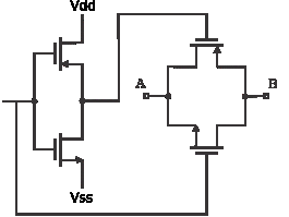
I´m developing a programable capacitor in CMOS 0.35um, but in the process I found some dificulties. What kind of mos switch do you indicate? I´m using a CMOS tranmission gate, but it´s not working. Thanks for your help.
PS: I want to show the figure but the forum don´t allow. I need 2 posts
 

You need to explain what "not working" means... Here you have a chance for a second post! ;-)
 
The "not working" means that the switch does not close the way. It´s like permiting to flow when that´s not desired.

---------- Post added at 17:58 ---------- Previous post was at 17:55 ----------

The figure.


If you are using transmission gates, check that the polarity of the control signals is correct, the bulk in connected correctly and that the input voltage is not higher than the control signal plus VT (the nmos would be conducting).
 
I´m using a transmission gate. The polarity is correct and the bulk of the nmos is connected to the gnd and the bulk of pmos is connected to the vdd. Is this the correct way? Thanks.
57_1294424449.png
 

yes, correct. What about the input and output levels wrt the vdd and vss?
 
The technology is TSMC 0.35um, using vdd as 3.3 V and vss as 0 V. The "not working" is like the switch and capacitor that is closed is consuming voltage.
 

I do not understand what you mean by consuming voltage but let's start from the basics: does it work correctly when you have only one switch (i.e. if the control signal for that switch is 0, the switch is open - non conductive - according to your figure in msg #5)?
When you have multiple switches in parallel, all the switches must be open to prevent the input to pass to the output.
 
In this circuit I want to choose one or more capacitors to make a diferent capacitance. This is the desired, when I choose 30 pF for the final capacitance the switch 2 and 3 (UP to DOWN) should close and the others open. But it seems that's not happening. My switch is wrong? The range voltage that flow through the switch is 0 - 2.56 V. How can I calc the better W/L for this task?
 
Last edited:

As I suggested in my previous post, run your testbench with one capacitor and one switch only, then check if it works. If it does, add one capacitor and one switch and try again.
Moreover, what is driving your capacitor and what is the load?


"not working" means that the switch does not close the way. It´s like permitting to flow when that´s not desired.

Are you aware that your circuit can work only if both In & Out do not float, but have a well-defined potential (GND - 0.5V) ≤ V{In, Out} ≤ (VDD + 0.5V) :?:
 
I´m using a transmission gate. The polarity is correct and the bulk of the nmos is connected to the gnd and the bulk of pmos is connected to the vdd. Is this the correct way? Thanks.
57_1294424449.png

I have another problem, when the switch is closed it's still conductive. I need it's set to 0V when closed. The input signal has the range 0 - 2.56V. How can I solve this? Thank you.
 

... when the switch is closed it's still conductive.
A "closed switch" should be "conductive" - it's its purpose!
But if you wanted to say "the open switch is still conductive", it is
  • either not correctly controlled
  • or defective
  • or it just looks like so, because the charge on the node can't disappear.

I need it's set to 0V when closed. The input signal has the range 0 - 2.56V. How can I solve this?

Put another switch (nmos only) between the node you'd want to set to 0V - and Vss. Control it by clk_bar.
 
I have done what you said, and when the switch is open it was set to 0V. But using this same switch in a switched capacitor the result wasn't good. The VSS in the switch act like a gnd and ground the capacitors. The circuit I'm working is like this. Where the box with numbers or letter are the switch.


... the result wasn't good.
That's a vague term. What's the pb.? Too much charge injection during switch-off? In such case, use the standard ½W/L compensation circuit.

The VSS in the switch act like a gnd and ground the capacitors.
That's what it is intended for, isn't it? At least when switched-on.
 

Hi guys, thanks for the answer. I misunderstood the functionality of the switch. Now I now how it works. And I have another question, if the amplifier used in the figure has the VDD = 3.3V and VSS = 0V, can I connect the positive input to the ground and the circuit still works as a integrator? (The amplifier is a folded-cascode)
Thanks.
 

yes, for single-ended operation.
But I'm simulating the circuit in this configuration and isn' t working. But if I replace the ground in the switchs and in the positive input for the VCM 1.65V it integrates. There is something wrong with my Folded-cascode OTA? Or this is the correct?
 

... can I connect the positive input to the ground and the circuit still works as a integrator? (The amplifier is a folded-cascode)

Depends on the input circuitry of your folded-cascode amplifier. Yes, if it has PMOS inputs.
 

Depends on the input circuitry of your folded-cascode amplifier. Yes, if it has PMOS inputs.
I'm using a NMOS input. So, if I use a PMOS input it should work with the grounded positive input? Or should I use the VCM = 1.65V?
 

Status
Not open for further replies.

Part and Inventory Search

Welcome to EDABoard.com

Sponsor

Back
Top