Continue to Site

Welcome to EDAboard.com

Welcome to our site! EDAboard.com is an international Electronics Discussion Forum focused on EDA software, circuits, schematics, books, theory, papers, asic, pld, 8051, DSP, Network, RF, Analog Design, PCB, Service Manuals... and a whole lot more! To participate you need to register. Registration is free. Click here to register now.

[SOLVED] How to calculate the input-referred offset voltage?

Status
Not open for further replies.

turtlewang

Member level 2
Joined
Nov 7, 2010
Messages
46
Helped
1
Reputation
2
Reaction score
1
Trophy points
1,288
Activity points
1,605
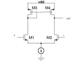
hello everybody, now i am designing a simple OPAMP for bandgap reference. I choose the following OPAMP. How can I calculate the random input-referred offset voltage? What I want is to use some equations to hand calculate the size of the input transistor, then use the calculated transistor for simulation e.g. Monte Carlo simulation.
Are there any documents describing the equation?
Thanks
 

Attachments

  • how_to_Calculate_offset.JPG
    how_to_Calculate_offset.JPG
    10.1 KB · Views: 235

For a simple hand calculation with the PELGROM equation you need a process dependent A(Vt) [mV*µm] value for the Vt mismatch from the foundry, or try a value to be found in literature: find a link to an appropriate IEEE paper in this posting!
 
The Avt can be found by looking into your process files for your technology. It is approximately the tox in nm = to mv. So example. If your tox is 9nm your offset voltage is 9mV for nmos, for pmos it is twice. So in calculating your offset of a differential pair(nmos inputs) you need Vos = (sqrt(2)*9mV)/(sqrt(W*L)) with W and L in um. So if your transistors is 10u/100n you put in 10 and .1 for W and L.

Hope this helps.
 
Last edited:
Vos = (sqrt(2)*9mV)/(sqrt(W*L))
A rather rough approximation, but quite good for an estimation. The Vos result value is valid for a 1σ (sigma) distribution. If your foundry delivers untested chips, you better calculate with a 3σ distribution, i.e. 3times this value.

BTW: The Avt=9mV*µm value is valid for a 0.35µm process (tox = 8..9nm).
 
The overall offset is a combination of the input-referred offset of the input pair and PMOS mirror:
Vos = Vos(input pair) + Vos(pmos mirror)
= Avtn / sqrt(Wn*Ln) + gmp*(Avtn/sqrt(Wp*Lp) / gmn

gmp*(Avtn/sqrt(Wp*Lp) is the current mismatch (gm*delta_vth) of the PMOS mirror, dividing by the input gm converts the delta-I to a delta-V.
Minimize the PMOS offset contribution by sizing the input pair gmn >> gmp
 
thanks all of you. All of you help me a lot! and I have found Avt and A_beta from the PDK documents. And I also find the equation from the book written by P.R.Gray.
Thanks again.
 

Status
Not open for further replies.

Part and Inventory Search

Welcome to EDABoard.com

Sponsor

Back
Top