jasonmgeorge
Newbie level 6
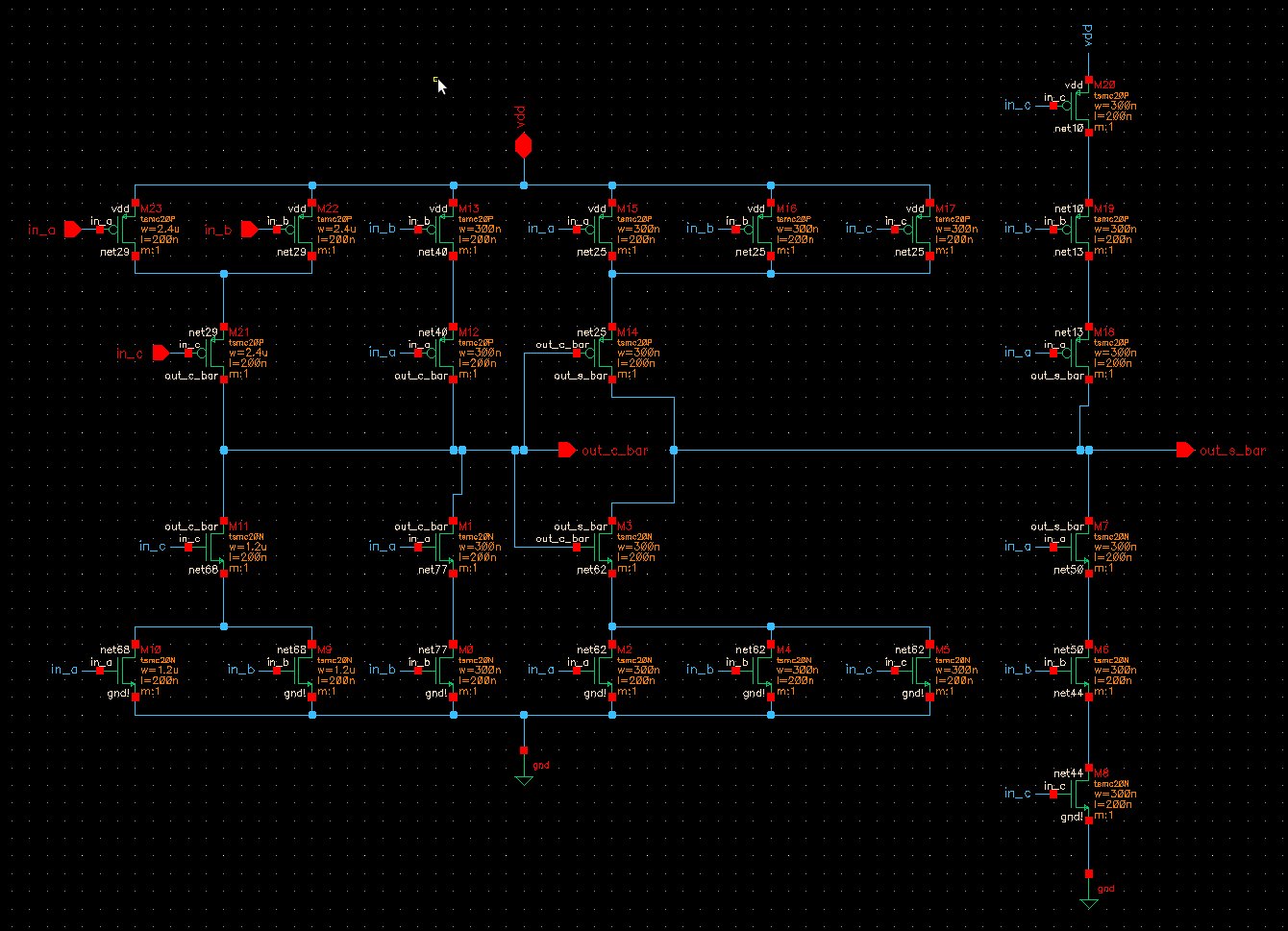
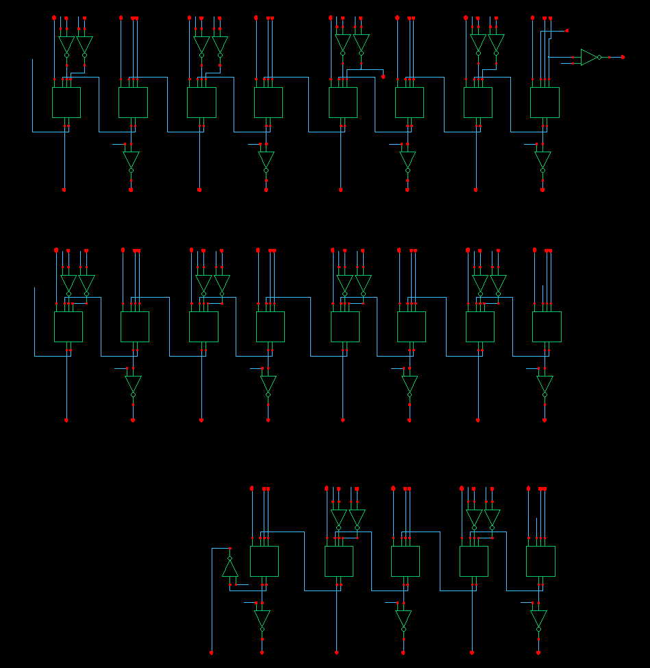
I'm having LVS trouble implementing a simple ripple-carry adder in Cadence. I'm building a 21-bit RCA using full adder and inverter standard cells I built previously. I have already used these cells in other designs without issue. For some reason with the RCA I'm getting "net-list ambiguities were resolved by random selection" for many of my A and B inputs that feed into the full adders.
termbad.out:
T -1 in_a0 / in_a0
? Terminal in_a0 in the layout is matched to terminal in_b0 in the schematic.
T -1 in_b0 / in_b0
? Terminal in_b0 in the layout is matched to terminal in_a0 in the schematic.
etc...
The nets appear to be correct in the extracted view. I've tried swapping the inputs in the layout, which still results in the same error message. Swapping the inputs in the schematic, however, correct the problem. The kicker is, not all of the inputs need to be swapped (bit 0 generates an error but bit 4 does not).
I've been pulling my hair out over this for hours now. Does anyone have an idea what this might indicate?