Continue to Site

Welcome to EDAboard.com

Welcome to our site! EDAboard.com is an international Electronics Discussion Forum focused on EDA software, circuits, schematics, books, theory, papers, asic, pld, 8051, DSP, Network, RF, Analog Design, PCB, Service Manuals... and a whole lot more! To participate you need to register. Registration is free. Click here to register now.

Nonoverlapping clock generation

Status
Not open for further replies.

andrea22

Junior Member level 2
Joined
Oct 1, 2010
Messages
21
Helped
1
Reputation
2
Reaction score
0
Trophy points
1,281
Activity points
1,427
Does anyone know how it works non-overlapping clock generator?
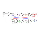
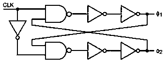
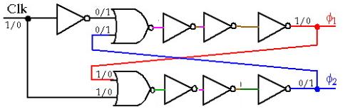
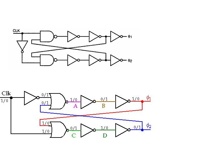
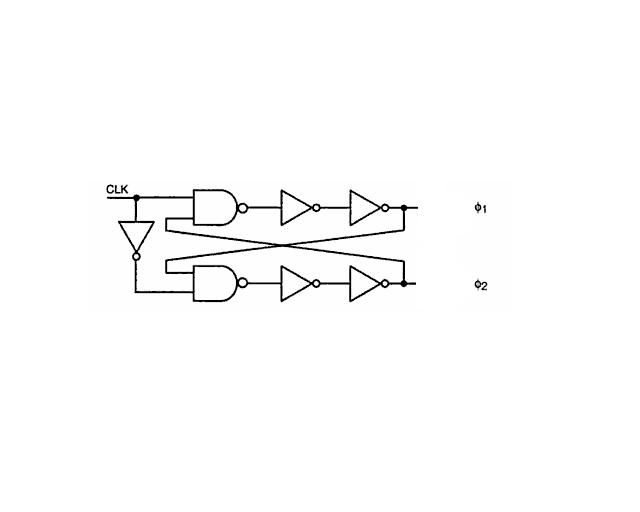
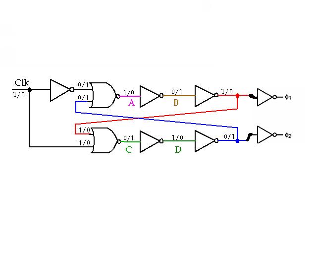
The circuit takes a clock signal and generates a two-phase nonoverlapping clock.
The amount of the separation is set by the delay trough the NAND gate and two inverters on the NAND output.
My question is:Why these clock signal must me non-overlapped?
How each logic gate (NAND and inverters) effects that those signals are non-overlapped?
How can non-overlapping time increase?
 

Attachments

  • generator.bmp
    960.1 KB · Views: 403

I forgot to say that all logic gates (NAND and inverters ) are realised in CMOS tehnology.
 

switched capacitor circuits need non-overlap clocks to control the switches well and avoid non-idea effects. refer to Allen's book on that chapter.
i put some ugly zeroes and ones on the schematic, the delay could be controlled by the delay element inserted between the output of one NAND gate and the input of the another NAND gate.
 

Attachments

  • generator.bmp
    410.5 KB · Views: 317
Ok,but why needed trhee invertrers to generate non-overlapping clocks?
Why when we realise non-overlapping cloks with NOR gates only two inverters are neeed?
 

Attachments

  • With NOR.jpg
    With NOR.jpg
    28.3 KB · Views: 366

you could run simulation and plot the waveforms of each node of interest, i think you can also get non-overlapping clocks at the nodes after two inverters with NAND gates, the duty cycle (maybe 55%) of the waveform is different from what you really want (let's say you want 45%) , so you add another inverter to invert it.
 

No,it can't with two inverters if you use NAND gates.
I tried that in PSpice.
With NOR gates only two inverters can generate non-overlapping clocks,with three it doesn't work.
 

59_1286108934.jpg

you meant this can not work? i havenot done simluation to verify, but it seems unreasonable.
what do you mean NOR gates with three doesnot work? like this ? i think it wont be working right
4_1286109175.jpg

anyway, 3-inverter is inverter, 2-inverter is delay
 

Yes,I ment that that can't work (with NAND gates)
The first circuit you posted works only with third inverter which is output of the feedback loop.(first picture I posted)

The second circuit works only with two inverters in feedback loop.(NOR gates).When I add third inverter it can't work.

I'm sorry if my English isn't so well,but this is not my language,so forgive me for mistakes in
writing.

---------- Post added at 15:03 ---------- Previous post was at 14:47 ----------


These two circuits work only this.

---------- Post added at 15:06 ---------- Previous post was at 15:03 ----------

This doesn't work:


---------- Post added at 15:14 ---------- Previous post was at 15:06 ----------

This also doesn't work:

I dont know what's the problem?
 

yep, the waveforms at the feedback node (2nd stage inverter) of the NAND gates version has high level overlap region so that the outputs of the last stage (3rd inverter) have low level overlap region, so you must add the 3rd stage inverter for this NAND version. and vice verse, for NOR gate version, you must remove the 3rd stage inverter.
non-overlap clock means the high-level voltage non-overlap.
 
Last edited:

So,in feedback loop,delay element (inverters) must be even number,
two,four,six....inverters must be used as delay elements,is that right?

---------- Post added at 15:47 ---------- Previous post was at 15:45 ----------

Why is that?
 

yes, even-stage inverters make delay element, no matter what version of the RS flip flop.
if you get high level overlap, just add one inverter to get non-overlap clock.
 
I need a 1 ns separation between the generated clocks, how can I increase the delay time, by the way I also use the CMOS tehnology
 

You can increase it for either style by just adding more
inverter-pairs (buffers), and for longer non-overlap by
interposing some RC network (or weak inverter plus dummy
load) in the delay chains. Active and passive approaches
each have their own sensitivities (P, V, T). How much
consistency you require will determine how elaborate
you end up, in the design (less than +/- 50% PVT may
require a stable reference with appropriate tempco and
maybe even a trim against process). Or, if you have a
master clock, you could make a replica DLL to get a
controlled-bias inverter to give you a fixed delay, at
a larger cost in complexity.
 

Thanks. Do you have any other suggestion on how to do this non overlapping circuit? Where one can control it with a different approach?
 

Status
Not open for further replies.

Part and Inventory Search

Welcome to EDABoard.com

Sponsor

Back
Top