dog2mari
Newbie level 4
- Joined
- Jun 13, 2010
- Messages
- 6
- Helped
- 0
- Reputation
- 0
- Reaction score
- 0
- Trophy points
- 1,281
- Location
- Seoul Korea
- Activity points
- 1,326
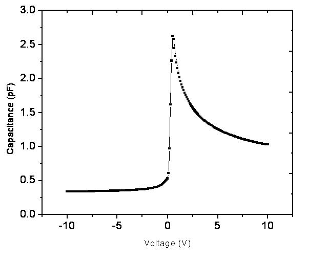
deep depletion...
could you explain it really really as in easy as even a child may understand?
could you explain it really really as in easy as even a child may understand?