Continue to Site

Welcome to EDAboard.com

Welcome to our site! EDAboard.com is an international Electronics Discussion Forum focused on EDA software, circuits, schematics, books, theory, papers, asic, pld, 8051, DSP, Network, RF, Analog Design, PCB, Service Manuals... and a whole lot more! To participate you need to register. Registration is free. Click here to register now.

how to choose device sizing for a TSPC edge triggered DFF?

Status
Not open for further replies.

mohamedabouzied

Member level 3
Joined
Feb 19, 2006
Messages
60
Helped
2
Reputation
4
Reaction score
2
Trophy points
1,288
Activity points
1,721
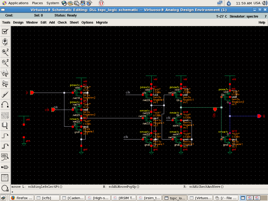
sizing tspc d flip flop

Dear all,
i don't know how to choose the device sizing for True single phase clock TSPC logic?
Especially, an edge triggered D flip flop DFF.

I put the transistors in its minimum sizing, but the DFF doesn't work, so i feel that i must size the transistors well in order to make the DFF functions well.

ANy suggestions?
Thanx in advance
Mohamed Abouzied
 

negative edge-triggerd tspc d-ff

Hi,

Which structure/topology you are trying to use?

give us the schematic so that we can..

Thanks,
 
tspc glitch

i have attached it
Thanx for your concern and fast replay

Mohamed Abouzied
 

cmos dff edge triggered

Why use minimum size transistors? As a thumb rule, in series path double the width of MOS. For more on sizing, read "logical effort"
 

dff,tspc,width

this is not cmos, logical effort doesn't apply. tspc doesn't seem to have a really sizing methodology, it all depends on the frequency you're operating at from my experience. for a given size, the lower the frequency, the less ability critical nodes have to store charge, the more chance of glitches and wrong results.
 

tspc cmos dff

Hi mohamedabouzied,

Still i m working out to frame a methodology for the kind of logic, but problem is charge sharing and coupling between branches, this directly results in glitch and current flow in both directions.

anyway coming to your design, I did a quick simulation with your topology using 130nm tech and it worked fine after this,

wp=3*wn, and make wn of m8 & m9 (2 nmos devices in second column) 2-3 times bigger than other nmos, this will ensure proper charging and discharging.

U can chose wn value based on your rise and fall time req., but remember u r clk slope will be critical for correct operation.

Hope this helps!!

Thanks,
 

Re: dff,tspc,width

this is not cmos, logical effort doesn't apply.

Not true; see the dynamic+domino logic chapters in the logical effort book. It also applies to pass-gate logic, although you have to think of the pass gate as part of whatever drives it. LE can even be applied to current-mode logic, although that's not in the book.

LE doesn't handle wire resistance well -- it only works if you can model wires as pure capacitors. It also ignores the gate-to-drain capacitance, so you do get increasingly-wrong answers for extremely-wide asymmetric stacks -- for example, the drive strength of a 32-input domino OR gate in real life will be much weaker than LE predicts since the dynamic node is loaded with 32 NFET gate-to-drain junctions. But I would avoid a gate like that in the first place...
 

Status
Not open for further replies.

Part and Inventory Search

Welcome to EDABoard.com

Sponsor

Back
Top