Continue to Site

Welcome to EDAboard.com

Welcome to our site! EDAboard.com is an international Electronics Discussion Forum focused on EDA software, circuits, schematics, books, theory, papers, asic, pld, 8051, DSP, Network, RF, Analog Design, PCB, Service Manuals... and a whole lot more! To participate you need to register. Registration is free. Click here to register now.

A strange zero comes at Enhanced miller compensation LDO

Status
Not open for further replies.

ckseu

Newbie level 4
Joined
Oct 25, 2005
Messages
5
Helped
0
Reputation
0
Reaction score
0
Trophy points
1,281
Activity points
1,310
when are rhp zero formed

85_1199669958.jpg
85_1199669958_thumb.jpg


42_1199669716.jpg


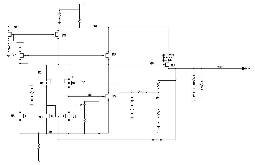
This structure is built follow the Rincon-Mora Enhanced Miller Compensation method
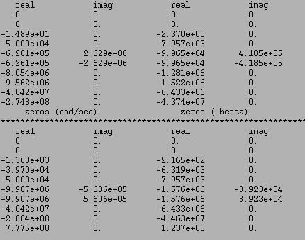
In his paper, the structure can pull two poles as far as possible. This loop can be compensated stably, But There is a zero=-2.165e+02, which I can’t find where it comes form. It seems too low. Cc2 have no effect to this zero. Cc1=10pF.
I hope to get help from the family of EDAboard. Any detail you want to know about the circuit please ask me.
Thanks!
There are two papers may be help :
Active capacitor multiplier in Miller-compensated circuits:

Dual-loop feedback for fast low dropout regulators
 
Last edited by a moderator:

miller compensated ldo

Hello ckseu,

The zero caused by Cc1, I think, would result in RHP zero because it provides a path to the output that is opposite in phase with the gain path through:M4, M9, and M0. The zero that you are seeing looks like a LHP zero which is probably giving you phase boost (and increased phase margin). What do you think about the zero formed because of the ESR of the cap at the load?

-Transbrother
 

compensation of ldo

Hi transbrother:
Thanks for your help!
It is right that the zero have relationship with the Cc1, because once I disconnect this loop the phasemargin is really down.
But because the Cc1 is 10pF only, I can not explain why the zero is at low frequency.
M3 is diode connected so output resistance is small,it seems no capabilty to inform the zero!
as to ESR, once I changed the value of Cload and Resr, the zero change a little but still stay at the frequecy nearby.
many thanks!
 

right hand side zero miller

Could you also post your bode plot?
Sometimes it is confusing to see just numbers without graphs and without the knowledge of what the unity gain frequency is.

I agree that removing Cc1 will lower your phase margin because you'll not be getting much pole splitting. However, I also think that the zero formed because of Cc1 is not giving you an increase in phase margin because it looks like a right hand plane zero.

1. Are you sure that the inductor and cap values are so high that they dont play role in the loop analysis?
2. When you measure phase margin and the loop, am I correct in assuming that you are looking at the feedback point. i.e. the other side of inductor connecting to the resistor?
3. Have you tried removing the ESR altogether, so there is no zero acting from the load?
4. What about the RHP zero because of the Cgd of the output device?


I hope these questions help.

-TransB
 

    ckseu

    Points: 2
    Helpful Answer Positive Rating
Dear transB:
Thanks again for your help,I confirmed for your Q1 & Q2
And I can not find a RHP from the p/z mapping I posted
for Q3, It does have effect to the zero, it shirt the zero about only one decade by varying the resr from 10m~1 ohm, so I think it not the domain factor to form the zero.

Another bad news I want to tell you, The circuit will oscillate on the -40'C~0"C under test. It may be occured a imagnary poles pair after Unit gain Bandwidth,and make the phase decease fastly.
may be it not a good method to compensation a LDO.

Best Regards
ck_seu@yahoo.com.cn

Added after 2 minutes:

Dear transB:
Thanks again for your help,I confirmed for your Q1 & Q2
And I can not find a RHP from the p/z mapping I posted
for Q3, It does have effect to the zero, it shirt the zero about only one decade by varying the resr from 10m~1 ohm, so I think it not the domain factor to form the zero.

Another bad news I want to tell you, The circuit will oscillate on the -40'C~0"C under test. It may be occured a imagnary poles pair after Unit gain Bandwidth,and make the phase decease fastly.
may be it not a good method to compensation a LDO.

Best Regards
ck_seu@yahoo.com.cn
 

HI ckseu
I ever have the same problem with you.
and I found this zero is formed by Cgd of the pass element(a large pmost in my circuit).may your zero is also be formed by this.Because the pass element is large ,Cgd can not be neglected.
 

Status
Not open for further replies.

Similar threads

Part and Inventory Search

Welcome to EDABoard.com

Sponsor

Back
Top