Continue to Site

Welcome to EDAboard.com

Welcome to our site! EDAboard.com is an international Electronics Discussion Forum focused on EDA software, circuits, schematics, books, theory, papers, asic, pld, 8051, DSP, Network, RF, Analog Design, PCB, Service Manuals... and a whole lot more! To participate you need to register. Registration is free. Click here to register now.

PTAT current source vs LDO to bias a ring oscillator for PVT insensitivity and power

doenisz

Junior Member level 2
Joined
Sep 12, 2021
Messages
22
Helped
0
Reputation
0
Reaction score
0
Trophy points
1
Activity points
315
I'm looking to minimize the frequency variation of an on-chip ring oscillator running at 2MHz, through using either an LDO as its supply voltage, or current-starving it with a current coming from a PTAT current source, coming from a constant-gm core

1713814645527.png


I simulated the ring oscillator with both structures having the same power consumption to make the comparison more fair. I generated the VREF for the LDO as a simple 2T voltage reference
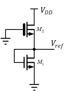
1713814704340.png
, because I'm on a power budget. Keep in mind, this circuit itself has some PVT and supply variation.

To my surprise, the PTAT current starving actually gave me better PVT insensitivity compared to LDO and I cannot really justify it with theory.

The only explanation I could come up with is that the resistance in the PTAT core tracks the PVT in the same way as the NMOS/PMOS in the ring oscillator.

I would appreciate it if you could please help me understand this better. I'd like to repeat, PTAT core and the LDO runs at the same power, so LDO bandwidth is not too great so it might be related to its settling too.

Best.
 
Bias that counters transistor behavior (such as PTAT
fighting gm (mobility) reduction w/ temp) can give a
better result than a fixed voltage (LDO, bandgap) if
you get the tempcos to "wash".

Whoever said "two wrongs don't make a right" never
did analog circuit design.
 
Bias that counters transistor behavior (such as PTAT
fighting gm (mobility) reduction w/ temp) can give a
better result than a fixed voltage (LDO, bandgap) if
you get the tempcos to "wash".

Whoever said "two wrongs don't make a right" never
did analog circuit design.

Good explanation in regards to cancelling what's happening with the transistors with a "non-ideal" biasing.

But the Vth of the transistors is also decreasing with temperature. And I simulated the ring oscillator running on an ideal supply voltage and its frequency increased with the temperature. The technology is TSMC 65nm RF LP. Transistors are HVT flavor.

So, the transistor tends to carry more current with increasing T, however, this would pull-down the source of the PMOS within the ring, I labeled it as VVDD below:

1713824306523.png


So, in my opinion, there's sort of a negative feedback action happening here, the more the ring oscillator wants to pull-down VVDD, reduction in VVDD counters this by keeping the VSG + VTP of the PMOS constant. Whereas with an LDO, we'd have higher Vov because VDD itself would be constant.

Thoughts?
 
There is a varicap effect on reverse bias PN junctions that reduces Cavg with Vdd so lowering the supply might offset the RdsOn which moves in the opposite direction of Cavg for Gate , Drain or Miller capacitance. I would expect series Rs and shunt Cavg to be the main factors of a ring oscillator and temperature sensitivity might be self-correcting this way with a current source rather than a voltage source for VVDD. I know that RdsOn rises with temperature, I forget how PN junction capacitance changes with temp.

(so much for my hand waving theory, maybe you can examine deeper.)

IDK but GPT says this...

The capacitance of a PN junction, often referred to as junction capacitance, typically decreases with an increase in temperature. This phenomenon can be attributed to several factors:
  1. Doping concentration: The doping concentration of impurities in the semiconductor material affects the width of the depletion region and, consequently, the junction capacitance. At higher temperatures, the number of charge carriers increases due to thermal excitation, which results in a reduction in the width of the depletion region and a decrease in junction capacitance.
  2. Carrier mobility: At elevated temperatures, the mobility of charge carriers in the semiconductor material typically increases. This increased mobility leads to a more rapid recombination of minority carriers in the depletion region, reducing the effective width of the depletion region and thus lowering the junction capacitance.
  3. Dielectric constant: The dielectric constant (also known as relative permittivity) of the semiconductor material decreases with increasing temperature. Since junction capacitance is inversely proportional to the dielectric constant of the material, an increase in temperature leads to a decrease in junction capacitance.
  4. Leakage current: At higher temperatures, the leakage current across the PN junction increases due to increased carrier generation and recombination processes. This increased leakage current can further reduce the effective width of the depletion region and thus decrease the junction capacitance.

Thank you. I actually use large mimcaps which dominate over the parasitic caps and, according to my design manual are quite robust against the temparature.

I also revised my simulations for mobility, vth, id and rdson and saw that id in fact decreases, and therefore, VVDD increases to pull Vov of the PMOS up.

So, it makes sense to me why the current source performs better than LDO for process and T.
 
One thing you would want to check is how your PVT corners are defined.
With your PTAT bias version, your frequency is a function of 1/(R x C x Vth)

In your process corner file, can you independently vary R, C and Mos corners?

Also, I am guessing here with the limited info, in the LDO version, you have a Ring Oscillator whose supply varies with the NMOS corners.
But assuming the Ring Osc frequency if it is based on charging from 0 to Vthn, has a period depending on NMOS corners, but the charging current is based on PMOS Vgs which will now vary all over the place since the Gate and Source are not tracking at all.

So your result would be expected.
 

LaTeX Commands Quick-Menu:

Part and Inventory Search

Welcome to EDABoard.com

Sponsor

Back
Top