Continue to Site

Welcome to EDAboard.com

Welcome to our site! EDAboard.com is an international Electronics Discussion Forum focused on EDA software, circuits, schematics, books, theory, papers, asic, pld, 8051, DSP, Network, RF, Analog Design, PCB, Service Manuals... and a whole lot more! To participate you need to register. Registration is free. Click here to register now.

[SOLVED] Bias T design

Status
Not open for further replies.

Zebxcore

Newbie level 6
Joined
Aug 24, 2022
Messages
12
Helped
1
Reputation
2
Reaction score
0
Trophy points
1
Activity points
256
Hello all,

I am fairly new into RF applications but I got some of the basic theory down. I have my first task for my company: Design a bias t with a bandwidth of 100MHz to 1GHz or higher (I was thinking 4GHz so I can use it for other testing purposes) with as low as an insertion loss as possible, 15V DC. But, this is my first time designing something that is so hard to get some knowledge on from books/websites/papers. Here is what I learned/know/done so far:

  • I am using a 50ohm input as well as output system.
  • Since my bandwidth is pretty wide, I learned that using cascaded inductors at different resonant frequencies helps reducing parasitic capacitances across the design.
  • DC blocking capacitor's resonant frequency should be far away from your signal frequency (Also applies to the inductors)
  • Coupling some resistors in parallel with the inductors helps take some of the parasitics as well.
  • Decoupling RC circuit in between inductors to help keep each inductor's SRF on check.
1661372735158.png

This is the basic design I made basing myself on one of the bias T's from mini-circuits (10MHz - 4.2GHz). However, L1 seemed like a ferrite bead rather than an inductor (I could be wrong). The values of the inductors as well as the decoupling RC circuits go from bigger to smaller from DC to RF path (L5 > L4 > L3 etc.).

I have two big questions and they are as follow:

  1. I am having issues picking the right inductance. Do you have to do trial and error for one inductance then split it into 3-4 inductors in series or pick an inductor value for each inductor? What about ferrite beads?
  2. For my given bandwidth, what would be the difference of an inductor having 90MHz SRF and a 1300MHz SRF? If most of my usage of the bandwidth is found between 200MHz and 900MHz I know a SRF of 1200MHz would affect me at or around that range, but would it be noticeable enough?
I also used this designed to guide me a bit better as to how these devices work and how each component interacts with other components https://www.qsl.net/in3otd/electronics/bias_tee/bias_tee.html

Edit: bad image, changed it. Added some more info
 
Last edited:
Solution
I was able to find why the power consumption was so high. Apparently, the cables I ordered to test this design out where not the same as the ones in the lab nor the devices we use to test, so I was inputting 5V into a data line with polarity protection. This caused the 5V regulator to act overcharge with current and fried itself.

Biasing looks amazing and return loss as well as insertion loss is phenomenal for low freq(400-900MHz), great bandwidth.

Thanks guys!
L1 is a Ferrite Core Inductor, no doubt. Bias Tee has not be so complicated, Coilcraft has some solutions for this purpose.

Minicircuits used these high valued inductors in order to down to very low frequencies but you don't need this.
Even any high valued inductor has low SRF, the target here is to get a high impedance.

For instance, when you do a simple Bias Tee with that inductor;
1661411701969.png

1661411733144.png

As you can see, the Insertion Loss is low and Reflections are pretty good.
 

i agree, that circuit is too complicated.
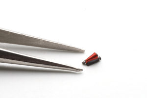
have you heard about Conical inductors?


at your low frequency range, i would find the cheapest connical microwave inductor, add some capacitors, and call it done!
 
Also you do a mistake in your simulation setup. A DC Supply cannot have 50 Ohm internal impedance therefore simulation won't be correct. A typical DC supply may have milliohm range internal impedance or basically it's assumed as short circuit for AC signals. Otherwise the simulation results will be pretty unpredictable.
 
Thanks for the heads up! This is my first time doing a design this way since I learned to do it in microstrip for higher frequencies and in more than ideal cases so it's basically brand new to me.
Untitled.png

Right now is looking something like this, I have been doing tons of research and ordered some samples for the 4310LC conical inductor to test out. So far, the model I made concurred with your results BigBoss so I am excited to test it in the lab.

If, let's say, I wanted to use the same design to power up and antenna at around 3Ghz. Would this design work? The one VNA we have its a really old HP that only goes up to 3GHz so I can do only enough testing.

Thanks again!
 

HMC636ST89ETR has its own application circuit that means components have been organized so that Output/Input Reflection will be good with them.
If you need a DC current at Input, you can use Bias Tee.
Nevertheless , you can try. Nothing happens.
btw: HMC636 is too expensive, If I were you I try yo use a single transistor amplifier with a appropriate designed circuit for a particular frequency ( 3GHz). You can obtain Lower Noise, cheaper and same Gain and OIP3.
Because using a very wideband amplifier connected to an antenna will amplify whatever up to cut-off frequency therefore using band-pass amplifier is much better.
 

Thanks again for the help.

My idea was to use two bias tee: One for the amp, another one for a remote piece of equipment on the input (left side). I have seen some chokes like the one above, but using different inductors so I wanted to make sure that everything, hopefully, goes as planned if I use the same inductor for both bias tee.

Right now, this design is going to be placed in a system that requires anything within 100MHz-2GHz to be amplified. I asked if it was usable in an antenna since I will be designing one next.
Also, I've been using the HMC636 since we already have a couple of them in the shop. But I get what you mean, using a bandpass amp seems to be the better option for an antenna.

Thanks again guys :)
 

Hey guys!

So I was finally able to do some testing, I ordered some cheap boards and got my hands to work. I found a couple issues to which I scrapped through datasheets to figure them out but can't seem to pinpoint the issue.
1664914782592.png
A little background: I wanted to use P2 (bottom connector) to power the board at 15V, providing 5V to opamp, attenuator, and dip switch to control attenuator, by using a resistive voltage divider (I should've use a voltage regulator though). However, I found that this bias tee was going to be incorporated to a system that provides 12V, 5V and 3.3V as well as I2C to control devices. So, in order to accommodate that implementation better, I used the 12V and 5V supply on board and the I2C to control the bias T.

Now, my issue comes to the amp drawing too much current from the 5V supply, making the inductor on the supply burning hot after a couple seconds. For reasons, I can't post the supply itself but its composed of a 12V input into a 5V regulator, out into an inductor and some more circuitry before hitting a series of multiple 10 pin connectors (6 connector for power, 4 for data).

I know this amp is suppose to draw somewhere between 150 and 170mA, but it requires close to 1A (about 850mA) just to get a jumpstart. Also, my 5V trace is grounded for some reason. Once I take off the amp from the PCB, 5V stops being grounded which makes me think that the output is being shorted to ground. Is this usual on this Amp? Do you guys have any other recommendations on Amps I could use? This one is not for an antenna but for various systems ranging from 100MHz to somewhere around 3-4GHz.

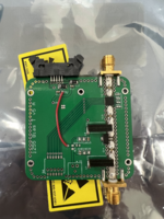
Tested the inductor on a separate board and worked just fine up to 4GHz, -10dB return loss at that point, then it goes close to -5dB after that. Insertion loss is pretty flat up to 4GHz as well, after that, I could see dips coming close to -3dB. That makes me think the FR-4 I am using might be the culprit since this board is super basic (inductor, 1uF coupling cap and 3 decoupling caps on DC trace on the back). I attach a picture of it as well.

1664916230814.png

Thanks!
 
Last edited by a moderator:

I was able to find why the power consumption was so high. Apparently, the cables I ordered to test this design out where not the same as the ones in the lab nor the devices we use to test, so I was inputting 5V into a data line with polarity protection. This caused the 5V regulator to act overcharge with current and fried itself.

Biasing looks amazing and return loss as well as insertion loss is phenomenal for low freq(400-900MHz), great bandwidth.

Thanks guys!
 

    andre_luis

    Points: 2
    Helpful Answer Positive Rating
Solution
Status
Not open for further replies.

Part and Inventory Search

Welcome to EDABoard.com

Sponsor

Back
Top