Continue to Site

Welcome to EDAboard.com

Welcome to our site! EDAboard.com is an international Electronics Discussion Forum focused on EDA software, circuits, schematics, books, theory, papers, asic, pld, 8051, DSP, Network, RF, Analog Design, PCB, Service Manuals... and a whole lot more! To participate you need to register. Registration is free. Click here to register now.

SPI Master with PSoC 5LP

Status
Not open for further replies.

wwfeldman

Advanced Member level 4
Joined
Jan 25, 2019
Messages
1,101
Helped
231
Reputation
461
Reaction score
297
Trophy points
83
Activity points
8,553
I want to use a Cypress (Infineon) Kit-059 to control a 16x16 cross-point switch, Analog Devices AD75019, using the SPI master component. The AD75019 takes 256 bits of serial data clocked in a CPHA= 0, CPOL=0 format. It then clocks the 256 bits in parallel to control the switches.

I am examining SPIM_Example Project 1.10 to get an understanding of using am SPI as a master. I am also looking at documentation component data sheets Serial Peripheral Interface (SPI) Master 2.50, Direct Memory Access 1.70, ap notes AN52705 and AN84810, and the data sheet for the AD75019.

I am tied down to the AD75019, as it is the only cross-point switch I have found with the appropriate voltage range. It gets a 256 bit data stream to set the 256 switches.

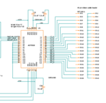
This is the portion of the TopDesign in PSoC Creator with the SPI Master
1655219920239.png

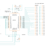
This is the pertinent portion of the crosspoint switch circuit, from Fusion 360 electronics:

1655220901945.png


in the SPIM Example, main.c:

CyDmaChEnable(txChannel, STORE_TD_CFG_ONCMPLT);

while (0u == (SPIM_ReadTxStatus() & SPIM_STS_SPI_DONE))
{
}

what I get, and do not get:
Does enabling the DMA channel cause it to transmit? If not, what does?
Where can I find the various codes, like STORE_TD_CFG_ONCMPLT, and what they mean/do?
The while loop continues through each 8 bytes of the buffer, until both SPIM_ReadTxStatus() and SPIM_STS_SPI_DONE are 1.

other items:
I am using the DMA because I need to transmit 256 bits. The SPI does 16 bit bursts, so I need to string together 16 transmit descriptors.

In operation, the crosspoint switch looks like an analog shift register, for at least 10 steps. (nothing, 8 steps, and nothing again)

Since I only want to transmit the data, as the cross-point switch is not an SPI device, but it does take serial data clocked in, in the same format as SPI ( CPHA= 0, CPOL=0 format.). I don't need the MISO input. The component sheet says it needs to be connected, but to what?
Is it okay to ground it, or tie it high?

Data lines selection "Bi-directional" looks more like what I need, and is what is in the schematic above: DATA and CLOCK.
Since there is only one SPI (not quite slave) device, I don't need the Slave Select, and plan to leave it unconnected.

The other question I currently have has to do specifically with the operation of the SPIM Example:
At the beginning of main.c, the data buffers are declared:
/* Data buffers */
uint8 txBuffer [BUFFER_SIZE] = {0x0u, 0x01u, 0x02u, 0x03u, 0x04u, 0x05u, 0x06u, 0x07u};
uint8 rxBuffer[BUFFER_SIZE];

How does the information in the transmit buffer (looks like octal(?) or hex(?) bytes 0 through 7) lead to the expected results per the SPIM example pdf? It is clear that Master RX data: is written directly to the LCD display.
(from the SPIM pdf file:)
Expected Results
The LCD should display:
Master Rx data:
090A0B0C0D0E0F

( I am thinking there is a disconnect between whoever did the example in PSoC Creator, and whoever wrote the .pdf)
 

Attachments

  • 1655220377480.png
    1655220377480.png
    25 KB · Views: 137
  • 1655220428375.png
    1655220428375.png
    77.9 KB · Views: 149

i am using PSoC Creator 4.4 with KIT-059

my question started out as "what am I dong wrong with the SPIM?"
that is, how do i transfer 256 bits correctly from SPIM in Kit-059 to crosspoint switch?

but i made a few modifications, and
during build, I got the following in output tab


HDL Generation...
Synthesis...
Tech Mapping...
Error: mpr.M0022: "Net_232" is not a top level pin. Not expecting internal three-state signals. (App=cydsfit)
ADD: mpr.M0037: information: Unused pieces of the design have been optimized out. See the Tech mapping section of the report file for details.
* C:\Users\Larry\Documents\PSoC Creator\LMA Amp Rack APNA Simulation\crosspoint switch test.cydsn\codegentemp\crosspoint switch test.rpt (Tech mapping)
Dependency Generation...
Cleanup...
Error: fit.M0050: The fitter aborted due to errors, please address all errors and rebuild. (App=cydsfit)
--------------- Build Failed: 08/11/2022 10:13:49 ---------------


and the only error in the report file:


Error: mpr.M0022: "Net_232" is not a top level pin. Not expecting internal three-state signals. (App=cydsfit)
Converted constant MacroCell: \SPIM:BSPIM:so_send_reg\ from registered to combinatorial
Converted constant MacroCell: \SPIM:BSPIM:mosi_pre_reg\ from registered to combinatorial
<CYPRESSTAG name="Global Clock Selection" icon="FILE_RPT_TECHM">
Digital Clock 0: Automatic-assigning clock 'SPIM_IntClock'. Fanout=1, Signal=\SPIM:Net_276\
Digital Clock 1: Automatic-assigning clock 'Clock_1'. Fanout=1, Signal=Net_30
</CYPRESSTAG>


questions:
1) what is mpr.M0022 ? (are error codes expounded upon somewhere?)
2) how do i find "Net 232" ? (or any other net?)
3) what is the actual problem that needs fixing ?

4) and while i'm at it, i need to get back to the SPI function
 

Attachments

  • crosspoint switch test.Bundle01.zip
    2.2 MB · Views: 115

Without opening your file (I need to wait until this evening my time to get on a machine that has the software) my guess is that you have a signal line to/from the SPI that is not connected to a GPIO port.
Susan
 

    wwfeldman

    Points: 2
    Helpful Answer Positive Rating
XP_data to SDAT has to be configed as a bidirectional pin

1660272069225.png


The interrupt is generated by the SPIM which triggers the TX_ISR scripts (if ISR has been enabled
in both SPIM and TX_ISR).

You find nets by cursor hovering over a route and right click, then properties. Sometimes Creator highlights them for you when you dbl click on error, other times you have to hunt for offending
net.

1) what is mpr.M0022 ? (are error codes expounded upon somewhere?)

Not sure about this, I would have to post on Infineon website to get that answer.


Regards, Dana.
 
Last edited:
@Susan - thank you
@dana - exactly right - XP_data to SDAT has to be configed as a bidirectional pin
i tracked it down by systematic deleting sections of the top design. when the error didn't go away, undo put that section back. on to the next section.

1) what is mpr.M0022 ? (are error codes expounded upon somewhere?)

i did post this on the infineon/cypress community - got the same answer you gave.

for my part, the most annoying thing is that it was bidirectional, and i changed it (and a few other things)
 

as noted above, i am trying to write 256 bits to an analog devices AD75019 cross-point switch from infineon (cypress) Kit-059.

the cross-point switch uses a serial data stream interface (data and clock). the cross-point switch does not (specifically) use SPI, so there is no chip select (ss).

i have been examining the SPI signals from the processor with an oscilloscope.

i have attached the current state of said project. the immediate goal is to get some output from the processor.
the next goal would be to get more data transferred, so ultimately get all 256 bits transferred.

there have been various incarnations over the last few days, (such as those described and attached above), none with any output at xp_data, nor has xp_ss ever gone low, and there is no xp_serial_clock output.

the output on the LCD display (photograph) shows the loop counter, j (3 = j) where the 3 cycles 0, 1, ... 5, 6.
the 0 on the next line is the k, which is not incrementing in the while loop - while (0u == (SPIM_ReadTxStatus() & SPIM_STS_SPI_DONE)). it did increment (continuously 0 to 65536 and repeat) in a prior incarnation that used the various DMA lines commented out.

a variant using three wires - bidirectional data lines instead of miso/mosi data lines also did not work (topic of post #2)

An attempt to transmit a few bytes, as done in "SPIM Example Project 1.10" also failed.

clearly, i am missing something (many things??)

so, a few specific questions:

1) since my slave component (AD75019) does not use the chip select (ss), but i need it connected, what do i connect it to? or is it sufficient to take it to a pin, so the requirement that it be connected appears to be satisfied?

2) what is missing in the configuration files?

3) what is missing in the main program to tell the processor what to transmit and when?

4) is there a better example to use as a guide?
 

Attachments

  • pulse test.Bundle01.zip
    2.1 MB · Views: 114
  • crosspoint switch 16x16 AD75019.pdf
    233.7 KB · Views: 132
  • LCD pulse test.jpeg
    LCD pulse test.jpeg
    160.8 KB · Views: 112

I would be inclined to just bit bang that interface, or if you need a
faster load do a schematic capture or Verilog 256 bit reg new component
and load then do a HW burst of it.

Inclination is do a quick bit bang, eval interface speed to see if acceptable,
and if not try following.

There are video presentations on creating component, start with symbol wizard
then either do the schematic capture approach and or Verilog.

Just as an example I did a Verilog (training myself as newbie) and all it took
for code was :

Code:
//#⋆theader
' id="MathJax-Element-1-Frame" role="presentation" style="font-size: 113%; position: relative;" tabindex="0">#⋆theader#⋆theader -- edit after this line, do not edit this line
// ========================================
//
// Copyright YOUR COMPANY, THE YEAR
// All Rights Reserved
// UNPUBLISHED, LICENSED SOFTWARE.
//
// CONFIDENTIAL AND PROPRIETARY INFORMATION
// WHICH IS THE PROPERTY OF your company.
//
// ========================================
`include "cypress.v"
//#end
' id="MathJax-Element-2-Frame" role="presentation" style="font-size: 113%; position: relative;" tabindex="0">#end#end -- edit above this line, do not edit this line
// Generated on 06/07/2020 at 15:00
// Component: SIPO64
module SIPO64 (
    output  reg [63:0] Para64Out,
    output  reg SerOut,
    input   ClkIn,
    input   ClrAll,
    input   SerIn,
    input   SetAll
);

//#⋆tbody
' id="MathJax-Element-3-Frame" role="presentation" style="font-size: 113%; position: relative;" tabindex="0">#⋆tbody#⋆tbody -- edit after this line, do not edit this line

    reg [63:0] SReg;

    always @(posedge ClkIn) begin

        if ( ( SetAll == 1'b1 ) || ( ClrAll == 1'b1 ) ) begin
  
            if ( SetAll == 1'b1 )
      
                SReg <= 64'hFFFFFFFFFFFFFFFF;                   // Set all bits in Shift Reg to "1"s
      
            else if ( ClrAll == 1'b1 )

                SReg <= 64'h0000000000000000;                   // Clr all bits in Shift Reg to "0"s

            end else begin

                SReg <= {SerIn, SReg[63:1]};                     // Shift right 1 bit and input the Serial in Bit
                Para64Out <= SReg;
                SerOut <= SReg[0];
            end
        end
 

//#end
' id="MathJax-Element-4-Frame" role="presentation" style="font-size: 113%; position: relative;" tabindex="0">#end#end -- edit above this line, do not edit this line

1660330557045.png


Note mine used a lot of resources as it was para out.


Regards, Dana.
--- Updated ---

You could also think about using DMA into a 32 bit SR component, burst that out,
do it again 7 times. Just a thought.

1660331751714.png


Regards, Dana.
 
Last edited:

Using bidirectional data pin is just inapproriate for your SPI application. I would switch to regular 4 wire SPI as a first step.

I agree with danadakk that you don't necessarly need the SPI master interface to implement your application, but it should work nevertheless.
 

Status
Not open for further replies.

Similar threads

Part and Inventory Search

Welcome to EDABoard.com

Sponsor

Back
Top