Continue to Site

Welcome to EDAboard.com

Welcome to our site! EDAboard.com is an international Electronics Discussion Forum focused on EDA software, circuits, schematics, books, theory, papers, asic, pld, 8051, DSP, Network, RF, Analog Design, PCB, Service Manuals... and a whole lot more! To participate you need to register. Registration is free. Click here to register now.

PMOS gate control

Status
Not open for further replies.

parth22

Member level 4
Joined
Mar 15, 2022
Messages
78
Helped
2
Reputation
4
Reaction score
1
Trophy points
8
Activity points
518
Hi all,
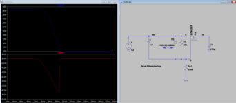
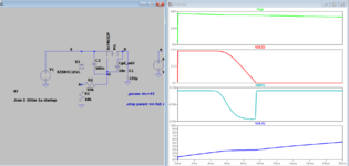
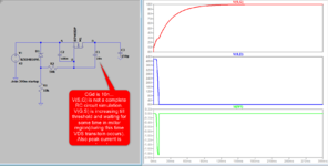
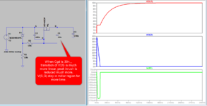
I have query regarding PMOS gate voltage. In the below image, everything is fine but if I change the supply voltage then VGS is changes and linear region of PMOS is going to be change.
Can anyone give suggestion how to control the gate voltage so it works in linear region for all supply voltage range (25-42).
Thanks.
 

Attachments

  • img1.png
    img1.png
    42.4 KB · Views: 115

Can anyone give suggestion how to control the gate voltage so it works in linear region for all supply voltage range (25-42).
What make you think it doesn't? Apparently you didn't perform a simulation for different input voltages.
Your specification isn't clear to me because you have posted different numbers in every inrush current limiter thread.

Charge time and peak current vary in fact with supply voltage. Peak current is roughly proportional to input voltage, so there's no problem at lower voltages. If the peak current is too high, you can change Rg1. There's also an option to use the zener diode to stabilize C charge current, but I doubt that it's even necessary. We would see clearer with a full circuit specification.

It's by the way not O.K. to use a schottky diode in place of D1, instead you should use a 15V zener.
 

Hi,

The circuit works like expectable.

So what do you expect?
Draw a diagram.

Klaus
 

What make you think it doesn't? Apparently you didn't perform a simulation for different input voltages.
Your specification isn't clear to me because you have posted different numbers in every inrush current limiter thread.

Charge time and peak current vary in fact with supply voltage. Peak current is roughly proportional to input voltage, so there's no problem at lower voltages. If the peak current is too high, you can change Rg1. There's also an option to use the zener diode to stabilize C charge current, but I doubt that it's even necessary. We would see clearer with a full circuit specification.

It's by the way not O.K. to use a schottky diode in place of D1, instead you should use a 15V zener.
Because in my circuit (in post 1),,,,maximum VGS is decided by (R1/R1+R2 )*42.....so if I change vin 42 to 24..maximum VGS is going to be changed...So
BTW i got it now,
thanks.
--- Updated ---

well it worked.
with the help of D1, you have fixed the VGS voltage to 15V.

I have one more doubt....if we go inside the MOSFET....
we see that when Id (drain current) reached it's on peak,,,,then VDS transition starts. or we can say time duration where VGS remains it's on miller voltage that time VDS transition occurs.
in the beloe pdf (page no 2)...we can see fig 2.

in the below simulation I can't see this theoretical behavior. Or I am thinking in a wrong way?

or it depends on application, in which region we want to transition of VDS?
 

Attachments

  • img9.png
    img9.png
    49.1 KB · Views: 91
Last edited:

Hi,

What does the 10nF do? I understand it's meant to be internal to the PMOS but wonder if LTSpice understands that as well (because I don't use LTSpice to simulate my circuits)...

In my innocence it looks like a 'self-turning off' circuit 'helper' via feedback, especially looking at your ID(M1) simulation results... Vg is gate voltage, V(S, G) is...? and ID(M1) - what's happening there, is it a pulsed input which is why Iout 'rises' and then 'falls'? - If so, then you've just created a single transistor 555 monostable/one-shot timer. VGS is controlled by V1 or what? - That's the why for your question in post #6, I guess.

These are serious questions. I'm just interested in your simulation results after seeing FvM's working solution.

So... you're saying that the input voltage is not what will control the gate voltage - VSD and VGS will be two different sources? Without looking at the PMOS datasheet myself, you'll know what VGS the part needs to be fully on and what gate current you will need to turn it on in whatever timeframe you require, and from there see if there's a logic gate (i.e. which family) that can output that amount of current or not, or will need e.g. a logic gate (if that's the gate control device you need to use for whatever reason) driving an NMOS or a BJT which will provide the required gate current for the PMOS pass device.

Page 1 of attached application note is useful (if you haven't already seen this one).
 

Attachments

  • DRIVING THE MOSFET QG and IG Microchip 00786a.pdf
    202.8 KB · Views: 81

Well, LTspice consider it as the additional capacitor.

it will help the more linear transition of VDS. As if the capacitor is large enough, it will take more time to discharge and VDS will fall down slowly.

V(S,G) is gate to source voltage of PMOS.
(Kindly have a look in the below images)

I am saying that as one will change the input supply voltage, final VGS will be changed.
 

Attachments

  • image_1.png
    image_1.png
    61 KB · Views: 72
  • image_2.png
    image_2.png
    70.9 KB · Views: 77
  • image_3.png
    image_3.png
    65.3 KB · Views: 77

    d123

    Points: 2
    Helpful Answer Positive Rating
Hi,

I use this capacitor to limit dV/dt during power up. Thus it also reduces the inrush current to the bulk capacitor ... and reduces stress (current peaks --> overshot, ringing) to the input power supply.

Klaus
 

    d123

    Points: 2
    Helpful Answer Positive Rating
Hi,

Super, guys. Thanks for the explanations. And, parth22, thanks for the nice, clear, comprehensible walkthrough examples to explain.
 

Status
Not open for further replies.

Similar threads

Part and Inventory Search

Welcome to EDABoard.com

Sponsor

Back
Top