cupoftea
Advanced Member level 5
Hi,
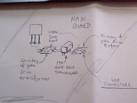
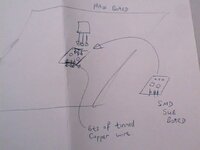
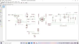
Doing 4kW SMPS.
There are heavy transformers and inductors, (~0.5kG) on the main board....so its going to flex a bit.....so all other components on this board will be PTH only.....no SMD as it will crack and desolder. Would you think the PTH will be ok?
Doing 4kW SMPS.
There are heavy transformers and inductors, (~0.5kG) on the main board....so its going to flex a bit.....so all other components on this board will be PTH only.....no SMD as it will crack and desolder. Would you think the PTH will be ok?