Junus2012
Advanced Member level 5
Hello
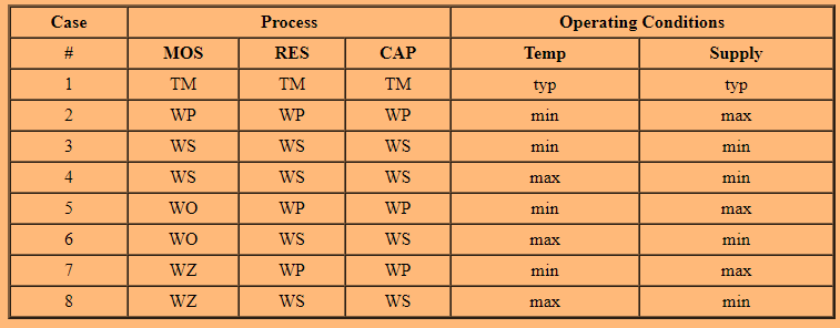
Below is the set of worst-case corners defined by AMS technology,

In reality, a huge number of the combination is possible making simulation with corners approaching the Montecarlo counterpart, in the other hand reducing the number of combination makes verification less realistic to the real.
AMS suggested the above table as worst-case ever condition, so validating design on this corner will assure the expected yield.
Here I am not discussing the accuracy of the above table, my question is that combination based on the AMS only technology or I can use this combination for any different technology
Thank you
Best Regards
Below is the set of worst-case corners defined by AMS technology,
| typical >(TM) |
| worst case speed > (WS) |
| worst case power >(WP) |
| worst case one > (WO) |
| worst case zero >(WZ) |
In reality, a huge number of the combination is possible making simulation with corners approaching the Montecarlo counterpart, in the other hand reducing the number of combination makes verification less realistic to the real.
AMS suggested the above table as worst-case ever condition, so validating design on this corner will assure the expected yield.
Here I am not discussing the accuracy of the above table, my question is that combination based on the AMS only technology or I can use this combination for any different technology
Thank you
Best Regards