Continue to Site

Welcome to EDAboard.com

Welcome to our site! EDAboard.com is an international Electronics Discussion Forum focused on EDA software, circuits, schematics, books, theory, papers, asic, pld, 8051, DSP, Network, RF, Analog Design, PCB, Service Manuals... and a whole lot more! To participate you need to register. Registration is free. Click here to register now.

RF Rectifier simulation and implmentation

Status
Not open for further replies.

myjoe1026

Junior Member level 3
Joined
Jan 7, 2016
Messages
26
Helped
0
Reputation
0
Reaction score
0
Trophy points
1
Activity points
198
Dear all,
I design a rectifier for 2.45 GHz in ADS with TXline and imported HSMS diode SPICE model.
1.jpg

With the LC matching, the simulation S11 is good.
2.jpg

When I fabricated the circuit, the result is not the same as simulation.
In fact, its efficiency is extremely low and the output DC volatge is 200mV(the simulation is 0.8V with RF to DC convertion efficiency 30%)
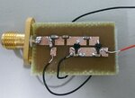
IMAG0704.jpg

I wonder where is the problem? TXline is 3mm for 50ohms.
Is that too wide for SMD capacitor and or diode IC?

Thanks for your reply.


When you use more stage of the Cockcroft-Walton the DC output voltage will be increase. I think you have a good result for the simulation. ADS software is so good, that is a pitty I am not use it.

- - - Updated - - -

I don't know what the diode you use (HMS 2852)? Have you compare the property of the component in the software and the real device?

Hi,

Yes, I used Avago’s HSMS-285x diodes. Is there any problem on my PCB layout(width should fit 0603 SMD or should be shorter or I should build some vias instead for black wire in the pic. to the ground)? I've imported SPICE model from the manufacturer, so let's believe the property of the components in the software are similar to the real device.
 

Hi,
Whay is your PCB material? Is it FR4?
 

> should build some vias instead for black wire in the pic. to the ground)?

Definitely!!!
Those wires aren't included in your ADS model and are a gross departure from the idealised ground connections shown in your schematic.

I've found achieving practical RF "ground" connections in a microstrip design such as yours to be quite challenging, especially with thick (~1.6mm) PCB. I've had reasonable success at 3+ GHz by paralleling two vias at each intended "ground" connection in a hand-made PCB, made by drilling 2x 0.6mm holes as close together as practicable (~1mm) and inserting short stubs of tinned copper wire, soldered top and bottom and trimmed flush with the cladding.

If you're going to remake your board, yes, I'd also reduce the copper pad sizes (represented by the MLIN's in your model) to the minimum dimension able to accommodate the 0603 SMDs. While ADS's empirically-derived numeric models for physical artwork are exceptionally good, they're not perfect and they're subject to assumptions made about the substrate. For a design made on a random piece of FR-4 fibreglass board without plated through vias, reducing the circuit geometry to the minimum size possible to diminish the [unintended] contributions of any distributed/stripline components will improve the agreement between simulation and reality.

Finally, be careful with the load presented to the output of your Cockroft-Walton multiplier. While they work well, they have notoriously high output impedances (always much worse than expected, in my experience!) and the output will droop badly when loaded with even modest resistances. I'd start at 10+ Kohms.

Good luck!

Oh, and the body of that SMA input connector *is* soldered to the plane on the underside of the PCB, isn't it? ;)

Hi,
Yes! The body of that SMA input connector *is* soldered to the plane on the underside of the PCB, which is the ground.
Thanks so much for your suggestion. I'll try those tips! Really appreciate that.
 

Hi,
Whay is your PCB material? Is it FR4?

Hi,
Yes, it's a 1.6 mm FR4. The top layer is as the pic. and the bottom layer is the ground.
 

The inductance in those ground wires are an obvious issue, drill some vias instead. I would redo the layout so the top side ground pour is much larger, and put many vias in it. Also I don't see L5 in your layout, though it may not be necessary.

I'm surprised your simulation is predicting a good S11, is that a small signal measurement? And 30% isn't too bad for a RF>DC converter. Keep in mind that high quality passive mixers have ~6dB conversion loss, which is 25% "efficiency."

Hi,

Thank you very much for the via suggestion, but I don't understand the meaning of " the larger top side ground pour, and put many vias in it." Do you mean draw a larger ground on the top layer and drill not only one via connected to the bottom layer ground? As for L5 and C25, they are matching network and soldered on the PCB. For simulation, I used a -6dbm source.
 

Status
Not open for further replies.

Part and Inventory Search

Welcome to EDABoard.com

Sponsor

Back
Top