Continue to Site

Welcome to EDAboard.com

Welcome to our site! EDAboard.com is an international Electronics Discussion Forum focused on EDA software, circuits, schematics, books, theory, papers, asic, pld, 8051, DSP, Network, RF, Analog Design, PCB, Service Manuals... and a whole lot more! To participate you need to register. Registration is free. Click here to register now.

contacts width in layout design

Status
Not open for further replies.

preethi19

Full Member level 5
Joined
Jun 30, 2014
Messages
273
Helped
0
Reputation
0
Reaction score
1
Trophy points
16
Activity points
3,474
Hi i am beginner in layout design and i am trying to design a layout for my circuit with reference to some examples i found. My doubt here is even if i follow the design rules for the contact what would be the correct way to place the contacts?? I know there is a minimum space, width rules that i need to follow. And in the image attached both the contacts on the poly follow the rules. Yet which is the better way to make the contact? Becoz in some examples i found the contact was just one and made big like the one below (but the poly length was less so the contact was bigger than the poly) and in some like 4 contacts together similar to the contact on the top poly in the image. If you say the above one is better could you also explain why. Is it just for the neatness of the design or is there any other factor to consider. Becoz in the end the contacts will be completely covered by the metal. Also say in above poly why do we have to use 2 contacts. Why cant i just use one on each poly and just make the connection. Thank you!!!
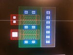
image (2).jpeg
 
Last edited:

Your foundry design rules will specify what size contacts you may use. Contact is one layer where they are very particular since contact to gate spacing is one of the dimensions that goes into determining a foundry's process node. (ie. 20nm, 15nm, etc).

Also, nothing is done for "just for the neatness of the design" though a "neat" layout is one indicator of a good layout.
 
Oh i understand now. dr.png
So from the image we can see contact size is 2. which is 2 lambda and the lambda value differs from technology. So i am working in 180nm and the lambda is 0.09. So 2 x 0.09= 0.18um. So my length and width of contact should be 0.18um. But i thought 0.18um was suppossed to be the minimum width and length that we can go down to and we can increase the dimension from der on. So contact size is fixed and not varying??? am i right?? Also then if the contact size is fixed why can't i just place one small contact on each poly and just connect it.. why do i need 2 or 4 contacts in one poly itself????

- - - Updated - - -

The reason i am got confused and thought that the contact size could vary is becoz for 180nm it is (2 x 0.09=0.18um). But i am working in cadence and i was seeing some examples of design already der having contact length and width of 0.220. It was more than the fixed 0.18um. So i thought we could vary the contact size..
 

Generally the foundry wants to pattern one size, not
variable. Although the one size may be different at
different layers.

If poly contact yield is a pain-point and you have a lot
of them, then contact redundancy costs very little and
can improve production yield significantly. In RF, gate
resistance is a big deal and driving that down by (say)
contacting both ends of the gate is common to see.
 

Oh so you say that by adding more contacts in one gate we drive down the resistance???? Is it right what i am understanding.. Please correct me if i am wrong... Thank you!!!
 

Marginally by more contacts at one end (if all are good).
Significantly by contacting at both ends. But if one is
bad, you sure wish you had two.
 
But could you please let me know what you meant by a bad contact or good one. Its just we place the contact on the poly to make a connection. How can a contact go bad if the placement is fine??
 

Realities of semiconductor manufacturing are superimposed
on your best intentions.
 

Status
Not open for further replies.

Part and Inventory Search

Welcome to EDABoard.com

Sponsor

Back
Top