bhl777
Full Member level 6
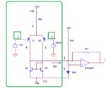
Hi, would someone help me in understanding the inverting and non-inverting nodes of the following schematic?
The input differential stage has an active current mirror, node 2 and 3 are the input nodes. node 2 has an DC+AC signal and node 3 is a pure DC signal as Vbias.
I am trying to find out which node is the inverting node and which one is the non-inverting node, but it seems like the explanation of different analog books are not the same.
This is my question:
1. generally we think the output node of the differential input stage is at the side of inverting input node. By this definition, since node 4 is at the same side of node 2, then node 2 should be "-", while node 3 should be "+".
2. However, it is clear in this circuit VS1 at node 2 is the input, while node 3 is just a fixed reference. So from the functionality node 2 should be "+", while node 3 should be "-".
How does this paradox happen? Thank you!
