kabaleevisu
Advanced Member level 2
- Joined
- Apr 14, 2010
- Messages
- 616
- Helped
- 85
- Reputation
- 170
- Reaction score
- 81
- Trophy points
- 1,308
- Location
- Chennai,India
- Activity points
- 4,512
Hi everyone,
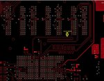
In my Board DDR3 section has some issue,Let me anyone give the solution.
DDR clock (Clk_0 & CLK#_0).Routed in top layer(Microstrip) because due to the less number of layer count.(Board has Eight layers)Four 4 DDR section used so, 64 Data signal occupied in two inner layer and Remaining layer for reference plane.Address and Clock are routed in Mictro strip only .I got feedback from SI team,Clock signal need to route in inner layer for avoiding radiation but if i followed those SI input, I need to increase the layer for clock signal for reference as well as clock signal has affect the enter path of data signal and I could not increase the layer count. I need to fix the problem so any one suggest the valuable solution to avoid the radiation in Top layer.
Attachments
Last edited:


