Continue to Site

Welcome to EDAboard.com

Welcome to our site! EDAboard.com is an international Electronics Discussion Forum focused on EDA software, circuits, schematics, books, theory, papers, asic, pld, 8051, DSP, Network, RF, Analog Design, PCB, Service Manuals... and a whole lot more! To participate you need to register. Registration is free. Click here to register now.

Layout problem . yellow warning - how to remove it?

Status
Not open for further replies.

AMSA84

Advanced Member level 2
Joined
Aug 24, 2010
Messages
577
Helped
8
Reputation
16
Reaction score
8
Trophy points
1,298
Location
Iberian Peninsula
Activity points
6,178
Hi guys,

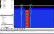
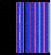
I am facing a problem here. You can see in the picture bellow:

8528899900_1418443984.jpg


I have join the drain and source of two transistor (diff. pair) in a interdigitated fashion. When I did this, cadence started to show a yellow warning.

I know that one can remove that but I don't remember how.

Does anyone knows?

Regards.
 
Last edited by a moderator:

If you just don't want to see it, just look at the list of layers in the LSW window and there should be named err or wrn or something similar and disable it. I remember something like this happened to me because cadence picks one side of the transistor as the drain and the other as the source; and when you do the layout, you connect a source and drain together and the warning appears. In reality, if the unit transistor is totally symmetric, it should not matter, and it should pass LVS. But since candece assign a drain terminal and source terminal, it may give you that warning. Maybe you can just try to mirror them vertically and see if the warning goes away. Note that you don't have the warning for the right part, maybe in that case you connected the terminal correctly from cadence's perspective.
 

Hmmm, those connections is for a diff. pair. I have connected them in a interdigitated fashion.

The configuration is something like:

A BB AA BB AA BB ... BB A

The first transistor (A) has is drain in the left. Then his source is connected to the source of the second transistor (B) then his drain is connected to the third transistor (second B) drain and so on.

The pattern then becomes something like drain - source - drain - source - etc.

Am I doing something wrong?

BTW, there is no option for that you suggested.
 

I recommend you to isolate the problem so you can figure it out if it is just a cadence thing or layout problem. Just create another cell with the diff pair only, do it aas you want and run lvs on the pair alone so you can see if the warning are not really that important.

Your layout plan sounds reasonable and it should work. Are you using pcells or creating your own transistors? Are you doing the layout by inserting pcells selecting from the schematic? Does kind of things make cadence think one transistor should be A but if you put it where a B transistor should go it gives you a warning even if you pass LVS because at the end the layout still is correct. So a strongly encourage you to isolate the problem to see if that warning can be ignored.
 
  • Like
Reactions: AMSA84

    AMSA84

    Points: 2
    Helpful Answer Positive Rating
I am using pcells by selecting in the schematic the transistor I want and then in the layout generate from the selected (...).

I think that I don't need to that because what I did in first place was to desgin the layout of the differential pair by selecting only those two transistors. Do you understand what I mean? It would be the same if I draw a schm only with the differential pair alone. Right?

For example, I started a few moments ago to design the layout of the active load of the diff. pair and only by joining the Source of transistor A with the source of transistor B (I remember that I have flipped horizontally the B transistor in order to put the S in the right position to join with the source of transistor A) that crappy warning yellow rectangle appeared!

I though that, because I am flipping horizontally the transistor B, I changed the order that cadence see the source and drain. This make sense? Don't know.

EDIT:

Picture 1:

9666244700_1418444191.jpg


Picture 2:


Another thing that I though, but is awkward(!) is that, because I am joining the S of MOST A with the S of MOST B (flipped horizontally) the NWELL (white) line will be super-imposed to each other.

If you notice in Picture 1, the warning yellow box starts at one limit of the NWELL layer of transistor B and stops at the other limit of the NWELL of transistor A.

Do you understand what I mean?

Don't know if it make sense!
 
Last edited by a moderator:

My suggestion to do the layout of the differential pair alone and compare it to an schematic of the same differential pair alone is to see if it passes. This would mean that you can ignore the warning, if you do LVS now it will not pass because you will compare the layout to the whole schematic, therefore it is more difficult to check if the warning is important or not.

If you are using pcells, cadence most probably will set the source and the drain. If you flip the transistor, the terminals will remain the same. You know that the source and drain can be interchangeable, but cadence does not know and the terminals will be set by the pcells. This should not be a problem to make a DRC and LVS clean layout if the warning is related to the terminals.

For the diff pair, the N-well is the same net so it should not give you any warnings/errors unless it is a DRC error.
 

I never found the generated starting layout much of a help.
Never liked flight lines and don't need the bogus flags either.
Are you sure you wouldn't be better off just laying it out by
hand?
 

Hi guys and thanks for the reply.

@scolis_GT
The layout that I am doing is from a 3-current mirror OTA. It is designed alone, in a separated schematic from the rest of the blocks - more, all the blocks were separated, that is, I did sub-blocks and in the end I have put them together. To do the layout I use each separated block (sub-block).

So this layout is being made apart from the rest of the other block.

However, what are you suggesting is to do only the layout of the differential pair, alone two transistors with the pins?

I notice that scolis_GT, that cadence puts the D and S. When I flipped the transistor horizontally, the D and S flipped too.

For the diff pair, the N-well is the same net so it should not give you any warnings/errors unless it is a DRC error.

It is a curious thing. This because, as you can see from the picture, when I just put together each transistor by the limit NWELL layer nothing happens. However, when I join the D with D and S with S, automatically cadence yellow box warning pops up.


@dick_freebird
It happens in the past, while in school, do the layout in that way. I done the layout by clicking on generate all from source.

Now, I am doing differently. I am picking each transistor from the schematic and put him in the layout separatly. I picked, for example, with the option: generate selected from the source (I think it is not the auto mode) the differential pair transistors and did the layout. Then the load from the differential pair, etc.

Any ideas? Maybe posting in cadence forum?

Regards.
 

I have similar problem!!!

As it seems, virtuoso doesn't merge Nwell as it merges PMOS's

However when I checked my CIW, I saw this warning
*WARNING* (DBAPP-2004): User-defined abutment function 'tsAbutFunction' returned an invalid offset keyword '6e-08'.
Valid keywords are 'top', 'middle', 'bottom', 'left', 'center', and 'right'.
 

Status
Not open for further replies.

Part and Inventory Search

Welcome to EDABoard.com

Sponsor

Back
Top