Welcome to our site! EDAboard.com is an international Electronics Discussion Forum focused on EDA software, circuits, schematics, books, theory, papers, asic, pld, 8051, DSP, Network, RF, Analog Design, PCB, Service Manuals... and a whole lot more! To participate you need to register. Registration is free. Click here to register now.
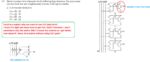
For the same drive strength, the NAND-NOT combination needs less silicon space than the NOR solution.
Vice versa, by using your NOR solution on the same silicon area as the NAND-NOT combination, the NOR output has less drive strength.
However, if you don't mind about drive strength (or silicon area consumption), your NOR solution is probably faster than the NAND-NOT combination, because it needs just 1 gate delay to achieve the result, instead of 2 propagation delays for the NAND-NOT combination.
Because the 2 PMOS in series - at corresponding W/L ratio - have much less drive strength for the logical 1 than the NAND's 2 NMOS in series for a logical 0. In CMOS, the NMOSFETs are much stronger than the PMOSFETs, for the same W/L ratio - about the factor µn/µp .
See explanations on Logical Effort, e.g. from here:
This site uses cookies to help personalise content, tailor your experience and to keep you logged in if you register.
By continuing to use this site, you are consenting to our use of cookies.