Continue to Site

Welcome to EDAboard.com

Welcome to our site! EDAboard.com is an international Electronics Discussion Forum focused on EDA software, circuits, schematics, books, theory, papers, asic, pld, 8051, DSP, Network, RF, Analog Design, PCB, Service Manuals... and a whole lot more! To participate you need to register. Registration is free. Click here to register now.

Help on this op-amp circuit

Status
Not open for further replies.

wizpic

Advanced Member level 3
Joined
May 23, 2004
Messages
789
Helped
108
Reputation
216
Reaction score
72
Trophy points
1,308
Location
London
Activity points
6,359
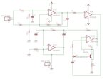
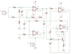
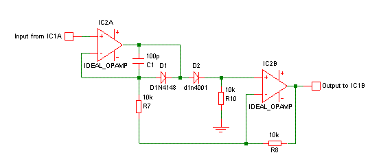
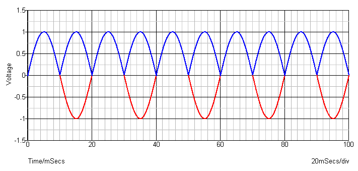
I have this circuit (Battery ampere hour monitor)and have a basic idea of how it works but would like to understand it a bit better. The principle of the circuit is that it's a bidirectional current flow monitor a 0-60mv signal comes in through X1 from 60amp shunt and it gets fed and amplified through IC1A then IC2A,B converts the signal to a positive value if the current is reversed. The part I'm un-sure of what is the purpose of R7,C2,D1,T1 and R10 does I presume it as something to do in converting the signal from a negative into a positive signal when the current flow is reversed ? . The rectified signal get's fed into IC1B. The output has a range of 0-1.8volts with 0-30amps current draw
Could someone please clarify this for me
 

Attachments

  • op-amp.JPG
    op-amp.JPG
    42.2 KB · Views: 80

It would be easier to figure out if you showed component values.

Anyway, the circuit shown won't work. There appear to be several mistakes in the schematic. For example, the inverting input of IC2A is not connected to anything, and C2 decouples the bottom half of the circuit from the top half, so there's no DC path. R4 and R5 look suspicious too. Are they supposed to be connected in series, with nothing connected to the mid-point?
 

Oh yeah sorry well spotted the corrected schematic is now attached I missed 2 nets off, R4 along with R13 are there for calibration values rather than a trim pot. I have yet got to add the values of the resistors as I wrote them down wrong on my drawing. Will get the correct values added soon.
 

Attachments

  • op-amp2.JPG
    op-amp2.JPG
    46.2 KB · Views: 76

OK, starting to get the hang of it:

IC1A at the input just converts balanced to single-ended and IC1B is a low-pass filter at the output, so the interesting part is IC2A, IC2B, D1, T1, and surrounding components.

Are the collecter and emitter of the transistor supposed to be connected together like that? If not, shouldn't there be something else connected to the non-inverting input of IC2B?
 

Are the collecter and emitter of the transistor supposed to be connected together like that? If not, shouldn't there be something else connected to the non-inverting input of IC2B?
Yeah that's how it is meant to be connected as this is what I thought at first but the circuit works but just curious what those R7,C2,D1,T1 and R10 do If I get time later I will have a probe around with a meter got to take wife shopping first
 

If you add the resistor values and send me
your Eagle schematic file...I'll run PSpise on it.

MAKeller
 

With the transistor connected like that, it's just going to behave like a diode.

I redrew the circuit as shown below to (hopefully) make it easier to understand, with the transistor replaced by diode D2.

According to my simulator, the circuit works as a precision rectifier. In the trace below, blue is the output, and red (partly obscured by blue) is the input.

The capacitor is presumably there to ensure HF stability of IC2A.

 
  • Like
Reactions: wizpic

    wizpic

    Points: 2
    Helpful Answer Positive Rating
Thanks Godfreyl.
I've been doing some more playing. It turns out when I looked close at T1 it turns out to be a Mosfet (2N3819) and not a transistor as I first thought(must remember to wear my glasses while reading) here is what I have put together and will try and explain it as best as I can.

With 25mv current flowing into the battery in on X1&2 with .73V on PIns 3&2 and 1.46V coming out of IC1A going into IC2A pins 3(+) pin(2) is 1.46 coming out of pin 1 is 1.67 then this goes onto the gate of the mosfet and at the other side of the diode there is 1.46V same voltage into IC2B and IC1B then a positive voltage out of IC1B. Then when current flows out of the battery there is a -25Mv going on X1&2 with -.73V on PIns 3&2 and- 1.46V coming out of IC1A going into IC2A pins 3(+) pin(2) is -1.46V coming out of pin 1 is 1.93V then this goes onto the gate of the mosfet and at the other side of the diode there is -1.46V then goining into pins 2&3 there is .01V and coming out of pin 7 (IC2B) there is +1.46V then a +1.46V coming out of pin 7 of IC1B. I do now have a better understanding of how it works and like the idea of a precision rectifier.

Would the mosfet still act like a diode with the Drain and source pins shorted ?

Thanks for taking the time to play and help
 

The 2N3819 is a JFET, not a MOSFET. It will act like a diode with the source and drain connected together. A MOSFET would simply act as an open-circuit.
 

Status
Not open for further replies.

Part and Inventory Search

Welcome to EDABoard.com

Sponsor

Back
Top