mtwieg
Advanced Member level 6
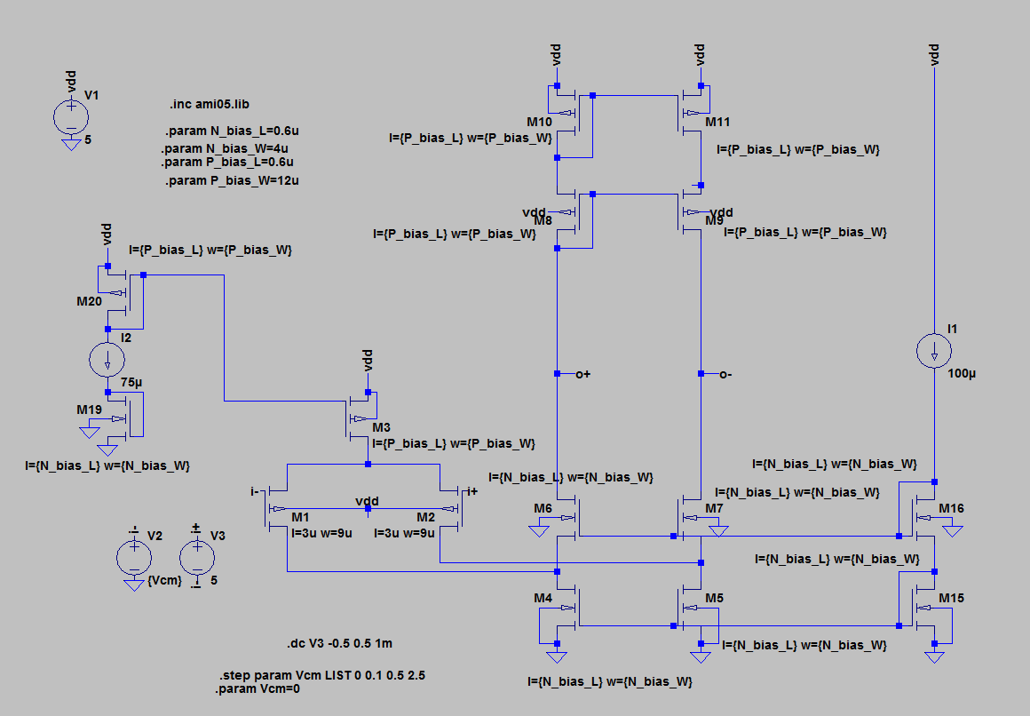
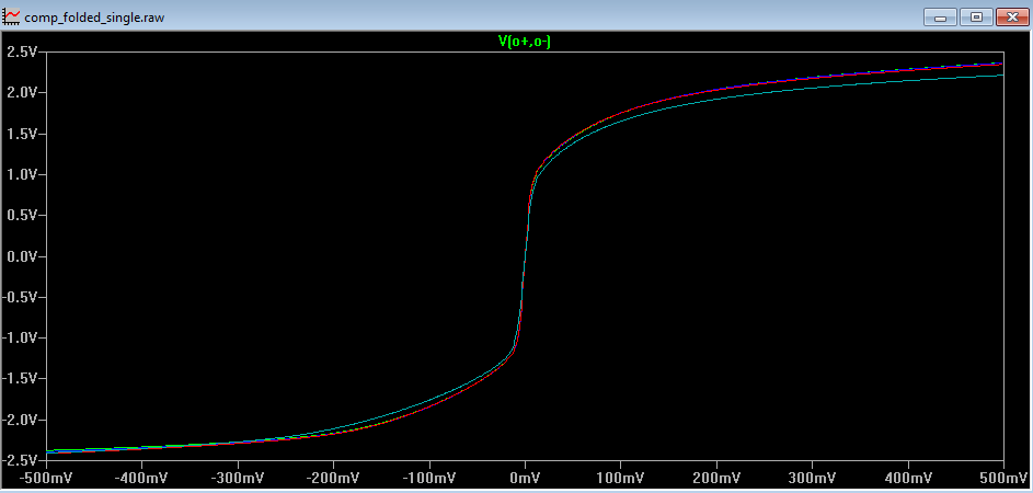
Hello, I'm currently doing my first "real" cmos design for fabrication (0.5um 5V onsemi). One of the main building blocks of my project is a rail-rail high speed comparator. I've done some rough simulations using a typical complementary input stage, and I find that it does work rail to rail, but the gain and speed are significantly reduced when Vcm is biased towards either supply (not just due to gm doubling at midpoint). When looking closely at the simulations, it seems that this is because some transistors are falling out of saturation (but not cutting off).
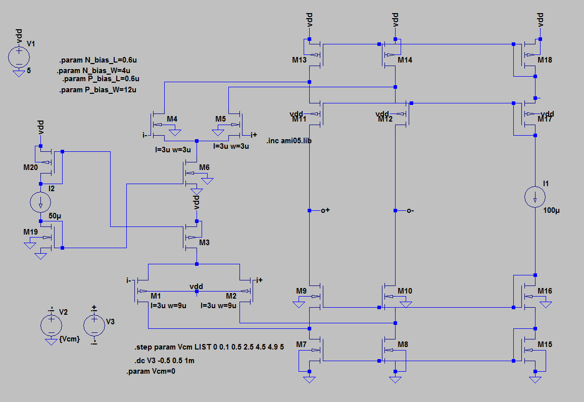
Rather than just randomly change sizes hoping for a working solution, I'm trying to approach this with some basic theory, but I'm not getting agreeable results so far. Here's a simplified circuit approximating the behavior of one half of a diff pair with active load. I sweep the input (V2) DC bias and look at the M1 and M2 operating conditions to see whether they are in saturation:
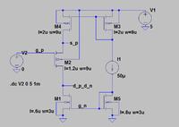
On paper I worked out that for M1 and M2 to both stay in saturation, I have to meet the following condition (I'm only interested in the low common mode input range limit for the P input stage):
Vin_min=VgsM2-VdssM2+VdssM1, which reduces to
Vin_min=Vtp-√(2*Ib/βp)+√(2*Ib/βp)+√(2*Ib/βn), which again reduces to
Vin_min=Vtp+√(2*Ib/βn)
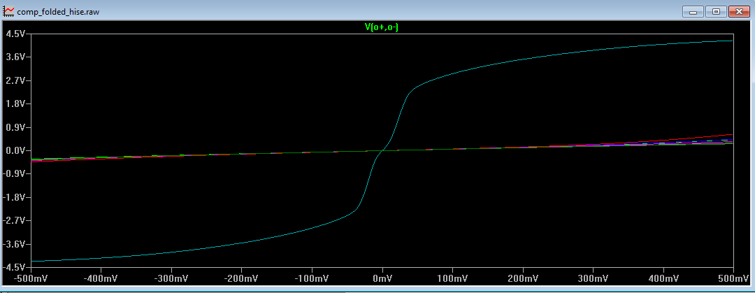
So I notice that is completely independent on the sizing of M2, and the Vth of M1. When I run the simulation though, I find that M2 drops out of saturation at higher than expected input voltages, and the biasing conditions don't match up very well with the basic equations I'm familiar with. At first I thought it might be body effect on M2, but if anything shouldn't that improve my input range by making Vtp larger (more negative)?
Is my approach just oversimplified, or maybe there's something wrong with my simulation? Any advice would be appreciated.
Rather than just randomly change sizes hoping for a working solution, I'm trying to approach this with some basic theory, but I'm not getting agreeable results so far. Here's a simplified circuit approximating the behavior of one half of a diff pair with active load. I sweep the input (V2) DC bias and look at the M1 and M2 operating conditions to see whether they are in saturation:
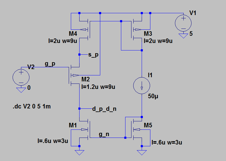
On paper I worked out that for M1 and M2 to both stay in saturation, I have to meet the following condition (I'm only interested in the low common mode input range limit for the P input stage):
Vin_min=VgsM2-VdssM2+VdssM1, which reduces to
Vin_min=Vtp-√(2*Ib/βp)+√(2*Ib/βp)+√(2*Ib/βn), which again reduces to
Vin_min=Vtp+√(2*Ib/βn)
So I notice that is completely independent on the sizing of M2, and the Vth of M1. When I run the simulation though, I find that M2 drops out of saturation at higher than expected input voltages, and the biasing conditions don't match up very well with the basic equations I'm familiar with. At first I thought it might be body effect on M2, but if anything shouldn't that improve my input range by making Vtp larger (more negative)?
Is my approach just oversimplified, or maybe there's something wrong with my simulation? Any advice would be appreciated.