Continue to Site

Welcome to EDAboard.com

Welcome to our site! EDAboard.com is an international Electronics Discussion Forum focused on EDA software, circuits, schematics, books, theory, papers, asic, pld, 8051, DSP, Network, RF, Analog Design, PCB, Service Manuals... and a whole lot more! To participate you need to register. Registration is free. Click here to register now.

Microstrip design of GaAs FET oscillator matching network many questions.

Status
Not open for further replies.

Terminator3

Advanced Member level 3
Joined
Feb 25, 2012
Messages
802
Helped
71
Reputation
142
Reaction score
63
Trophy points
1,308
Activity points
9,027
I am learning example from book "RF Circuit Design Theory and Applications", second edition, Reinhold Ludwig, Gene Bogdanov p.476 "Microstrip design of GaAs FET oscillator".

On the page 471 there is oscillation condition formulas:
k<1 - stability factor must be less than unity.
Гin x Гs =1 (condition 1)
Гout x Гload =1 (condition 2)

on page 473 said, that if oscillation condition met either at input or output port, the circuit oscillates at both ports... Does it mean if i make matching network on drain, but gate will be not matched, there would be an oscillation? But how frequency is determined in this way? When both port are matched to Гin x Гs =1 and Гout x Гload =1 conditions, i can guess that because both ports electrical matching stub lengths related with frequency, then it is clear about frequency of oscillation. What if on of ports matched to other frequency.. This is my first question.

fet-dgs-ask-1.png
QUESTION N2
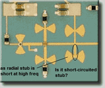
on the image we can see oscillator from www.ltcc.de

2.1. Why gate stab is a little longer, than half-wave? As i understand gate stub here is microstrip resonator. As it is longer, that means to me lower frequency of operation. And varactor can make it even much lower.

2.2. In question N1 source stub is used to increase instability, making k very small. That stub was < lambda/4 and short-circuited termination. But look here, source stub is longer, than quarter-wave. For short-circuit termination this source-stub will be a Capacitor, and only for oupen-circuit termination it would be a Inductance. So what purpose of that stub? Is it short-terminated or open-terminated?

"?" thin strip on gate looks as GND via.

fet-dgs-ask-1.png
Question N3
What is the length of gate microstrip when we using DRO? There is some position where DRO is placed, but stripline is always longer. I can't understand how to determine that length.

Question N4
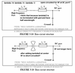
here is the image:
fet-dgs-ask-2.png
is it? Or not? I thing it is at High Freq (lambda/4 freq).

Question N5
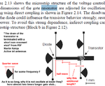
again resonant gate stub problems, why length vary so strong? Why not lambda/4?
fet-dgs-ask-3.png

Thanks! More question pictures coming soon =)
 
Last edited:
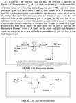
Given that most folk might not have the same book, we might not be able to respond in very specific manner. There are some things that may apply.

Regarding oscillation at both ports.
The device is between the ports, with also some matching items in there. The whole arrangement has gain (S21), and cannot oscillate without. If it is oscillating at all, the oscillation will be present at both input and output ports. It is a necessary condition connected by S21. It is something you expect.

Regarding the unexpected stub lengths. These of course vary with the Er dielectric constant of the substrate, but many times when using a stub, one does not make it exactly quarter wave electrical length. To deliberately have be of a inductive or capacitive nature, one might want to make it longer or shorter. If being part of the components determining the oscillation frequency, then it might well have to be apparently a "wrong " length to compensate for the presence of all parasitic and other unavoidable physical bits, (eg. bias, etc.).

I do not have opportunity to comment more right now.
 
A few things one must know to understand in those circuit layouts, and to allow one's mind to grasp certain concepts:


(1) What is the length of a quarter wavelength (QW) line section given the er (epsilon sub r, relative dielectric constant) of the substrate you have. This will help to determine the function the designer intended for various line sections (matching, isolation via QW stub 'tricks', Bias, etc).

(2)The "winged" things are (must be) capacitors to ground. One QW (quarterwave) back from a capacitor (a 'short' to ground) will exist a high impedance; if this length is shorter than QW on the substrate then electrically it will be *inductive* at the 'open' (or opposite) end, if longer it will have capacitive reactance . Often DC bias lines to the Gate and Drain use various QW structures to 'deliver' DC to the active device and to do so without affecting (decouple from) the RF characteristics.

(3) In any oscillator, there should be only *1* structure that determines the oscillating frequency; all other structures are matching, Gate and Drain DC bias and/or isolation structures, or RF ground structures (like Source to ground or RF ground) or the intended 'fedback' (sometimes designs rely upon internal device parasitic capacitances to provide the 'feedback' path)


Darktrax had some good points, so re-read his post with my points in mind too.


RF_Jim
 
Can i rely on the length of radial stub to determine lambda/4? I just use it radius directly as lambda/4, because everywhere is written so. Using this approach i hoped that i can know real microstrip electrical lengths without knowing substrate Er. I have some doubts about radial stub: for example, from which point measure it length. I can measure its length from the center of microstrip it is attached to, or from the side of that microstrip. Looking at "current view" results in EM simulation i think the second way is right, because in that case reflected wave can-not "influence" center wave propagation of the main microstrip. But also it is my doubt.


The "winged" things are (must be) capacitors to ground. One QW (quarterwave) back from a capacitor (a 'short' to ground) will exist a high impedance
RF_Jim, is it about drain "winged" things or source "winged" things? Or both of them..
View attachment 90130
I am not understand why QW stub becomes capacitor. If it's lenght exatly one QW, impedance is 0 and it is short circuit. Does it mean that that radial stub is a little shorter than one QW, so it becomes capacitive, with very little capacitance? I have doubts about how to analyze such things one-by-one: for example on the picture above, if i go from drain microstrip downwards through QW line, i obtain zero impedance, and winged radial stubs attached at zero impedance point (short at high frequency point) acts as capacitor, because maybe it's length is a little smaller than one QW..

For example, here is example from one paper:
radial-stub-ask.png
i can't understand why QW areas are inductance L?

I have such doubt:
radial-stub-ask2.png
is that right?
two lambda/4 sections to VCC forms lambda/2 line, wich have very big impedance for HF, and open-circuited?
then we add radial stubs at short-circuit poistion to short-out HF. But because full length of lambda/4 line + radial stub lambda/4 gives open circuit again, that radial stub have less influence on main transmission line. Right?
 
Last edited:

I do so like the term "winged things" meaning radial stubs - I can't stop myself from using it now :)

BUT.. It is very important we all understand what the winged things do, and especially, why we place them as we do. The radial stubs are RF short-circuits that are still DC-open circuits. They do the same job as capacitors to ground, but with some special extra properties.

They work slightly differently depending on the purpose and thickness of the line the are applied to.
A quarter-wave microsrtip stub that is part of a tuned circuit, or a matching section, when optimum, may well be a short fat thing. It may well have impedance much lower than Zo.

To be able to sweetly ground it without involving a big wide TEE that may itself end up being a major player, with a side component that complicates the resonance and might introduce new ones, a radial stub (or two!) allows a well defined shorting point. The radial impedance is wider band, very quickly getting ever lower down the radial. You avoid a large distributed TEE junction. Winged things are wideband, and very useful. Simulators usually allow the radius, and the angle to be "tuned" to opimise the grounding, but they are not supposed to be a major part of a tuned stub length, though I can imagine some might have explored using a radial stub as the whole resonator.

Putting two quarter wave lines, shorted in the middle with winged things, is a great way to introduce a DC bias voltage. The first can be the width for optimum match, or oscillation, whatever. The second can be thin, so high impedance, and by the end of the second line, there is no RF left at that frequency, and one can use a lumped capacitor to decouple, and further tracking is DC rules only.

If you cannot sneak the DC bias up a stub that is already doing duty in some other way, then two thin lines with a winged thing between, can be the way to bring in the bias, without the other microstrip lines being hardly affected at all.

These things are illustrated in the image attachments. The last image clearly shows lambda/4 line with "winged things" shorting, then into another line, ending on a lumped capacitor. The second from last image shows a 2-line bias structure from the top, and a resonant stub below, both connected at the same place on a transmission line.

- - - Updated - - -

With acknowledgements and props to the Microwaves101 folk, here is what you may expect from "winged things" (Radial Stubs)
stubcomparison1.jpg
stubcomparison2.jpg

To check if radial stubs are useful at your frequency of interest, and with the substrate you have in mind, you might need to simulate for yourself, changing the scenario to suit. At lower microwave frequencies, they may end up too large to be useful.
 
A quarter-wave microsrtip stub that is part of a tuned circuit, or a matching section, when optimum, may well be a short fat thing. It may well have impedance much lower than Zo.

As i know, quarter-wave stubs can be attached at two places:
first place: attached directly to main transmission line, to stop frequency at f@lambda/2 or make RF ground for varactor.
second place: to biasing line, that i can't understand earlier
When you write about "short fat thing", is it only theese two cases, or there are more of them?
 
Well stated Darktrax.

- - - Updated - - -

I am not understand why QW stub becomes capacitor.

Have you been introduced to, or make use of the Smith Chart in your education (or job) yet? The Smith Chart is instrumental in understanding the "impedance transforming" properties of lengths of transmission lines, the most important 'length' being the "quarter wave" (QW) line, since this can 'transform' low impedances to high impedances.

Also, variation of QW line 'stub' length (in this case, I mean 1 QW away from a connection directly to ground) makes it's impedance reactive, either capacitively (longer than QW) or inductively (shorter). This can be handy for adding one of those quantities to the circuit for various purposes, such as impedance matching.

It is critical at this point that you understand how changing line lengths changes (transforms) impedances, and the Smith Chart is a graphical aid that allows one to see the change in capacitive or inductive reactance quantities for changes in line lengths.

Circuity of the type under consideration in this thread, MMICs (Monolithic Microwave Integrated Circuits), make use of these line Z transformation 'tricks', so one must become intimately familiar with them, and the Smith Chart.
 

I want ask some questions. Some papers like to say, that they use f0@quarterwave stub to reflect f0 back somewhere. When i read this i think it is wrong, because quarterwave stub is attached to transmission line at 90 degree (geometrical placement, not phase). Or there is really some reflection exists? I did not saw any in sonnet lite simulator.

I can believe, that such quarterwave stub can reflect something back, but only if it have some other degree, for example 45 degree, as in DB6NT frequency doubler:
https://www.edaboard.com/threads/273639/
there is "X" section, that reflects LO to LO and doubled to toubled area and also cancels it.
View attachment 83953

Also i read two papers, where stated that frequency can be reflected by band-pass filter. When used in harmonic oscillator (oscillator where we want only second harmonic), such band-pass filter at 2xLO somehow reflects LO back to active device and make it to be "reused" to maximize second harmonic output. I searched on this topic and found some information, but still not understand clearly where to put band-pass filter exactly from the active device, to increase harmonic output.

- - - Updated - - -

RF_Jim, i tried to make various real PCBs with NE3210S01 fet transistor. Most results was unsatisfactionary. So i started to investigate why in this topic: https://www.edaboard.com/threads/286013/
You gave me a good idea to review that program to play with smith chart and stub lengths...
 

When you write about "short fat thing", is it only these two cases, or there are more of them?

Not at all only these two cases. Use it whenever the frequency is so high that lumped component capacitors to a pad with vias is no longer suitable. You may find that radial stubs is not good enough without being inconveniently large. It depends on the frequency you need.

PTFE-glass and ceramic-loaded PTFE substrates with Er from 2.2 to perhaps 3.5 may not be so well suited as for thin Alumina where Er=9.8, delivers a much more effective short from a radial stub. In these constructions, radials become more useful. My experience does not extend to MMIC, but I think that, in any smaller construction like on GaAs, radial stubs may be the only convenient way.

Re: "Short Fat Thing". Typically, in the matching circuits up to an active device, you can use series strips of differing lengths, with shunted strips going to ground short, or open circuit stub made lambda/2 which will move the input impedance over the Smith Chart to a wanted point. This might be the point of best gain, or lowest noise, or some compromise. The widths of the shunt strips may well end up to be so wide, they exceed the length. It is quite awkward then to make an effective short to ground.

_____________________________

At this stage, from the nature of the questions, we are getting into how transmission lines work, and where "reflections" come from, and how they affect impedances. These are things that need to be well appreciated before attempting to design microwave oscillators that use a deliberate open stub on a FET source to guarantee the needed instability!
It need not take too long to learn, and I am sure there are many good explanations and links in this forum on that subject.

Good oscillator design gets to the very limit of my knowledge, and we should much respect those able to do it well.
 
Last edited:
Question about DRO placement:

For exmaple, In Series-feedback oscillator DRO placed near gate microstrip. From some googling i found out, that electrical length from FET gate to DRO is about 180 deg. (some online patent) Why? Is it necessary to wave come-back in-phase (180+180=360), or some other purpose? Actually a read many papers, googled for many PDFs: there are DRO, ring resonators, spiral resonators, rectangular "ring" resonators, etc. all placed in some distance near gate microstrip, but none of papers mention at wich distance and why.

I can understand what going on in parallel feedback DRO: it is necessary that electrical path from drain to gate was about 180 deg, then assuming FET phase shift is 180 deg too, there would be in-phase waves on gate (180+180=360). But in case of series feedback it is not so obvious. There are some equivalent schemes of DRO using LRC elements, but i do not understand how to obtain that distance (along gate microstrip) where DRO is actually placed.

for example, in this paper: **broken link removed**
Series feedback configurations are based on the ability of the active device to produce a negative
resistance (reflection coefficient greater than 1) at at least one of the three terminals, in the frequency
range of The small signal oscillation conditions in this case arc reduced to:
|S| x| Г| >1
angle(S)+angle(Г)=2*Pi*n
where S and Г are the reflection coefficients of the transistor(S) and the resonator(Г) at any plane between
the device and the resonator (Fig. 7a). Since Г is always less than 1, this condition implies that
S looking into the device should be greater than 1. A distributed capacitance in thc source for the
configuration of Fig, 7a and inductance in the gate for the configuration shown in Fig. 7h is commonly
required to generate a high value of lS11l (> 1). Position of the dielectric resoriator with respect to
the device is now determined to satisfy the oscillation condition completly.
i do not understand ho to use it practically, where i can get Г coefficient of resonator

upd: found some lectures: **broken link removed**
write later if still do not understand...
 
Last edited:

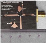
Maybe someone clever clarify this for me:
spurline.jpg
For example here, how the spurline part must be analyzed? In calculations even 0.01mm have big impact on frequency, how to think about such stuff..
 

Status
Not open for further replies.

Part and Inventory Search

Welcome to EDABoard.com

Sponsor

Back
Top