Continue to Site

Welcome to EDAboard.com

Welcome to our site! EDAboard.com is an international Electronics Discussion Forum focused on EDA software, circuits, schematics, books, theory, papers, asic, pld, 8051, DSP, Network, RF, Analog Design, PCB, Service Manuals... and a whole lot more! To participate you need to register. Registration is free. Click here to register now.

Op-amp offset voltage changing highly with T

Status
Not open for further replies.

Junus2012

Advanced Member level 5
Joined
Jan 9, 2012
Messages
1,552
Helped
47
Reputation
98
Reaction score
53
Trophy points
1,328
Location
Italy
Activity points
15,235
Hello

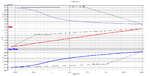
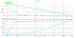
I am simulating one OP-amp. the op-amp should perform with temperature range from -25 to 80 Co.
I have found at some corners in the worst case analyse that the offset voltage is changing hardly with T so the gain is being killed, while it is stables at the other corners.
I dont know whether I should consider the design is failed or not ?? ??. some friends told me that it is ok to have offset voltage changing high with T but I am thinking then what is the meaning of this test with T?.

Note: the test is performed under open loop condition

I am also looking for your opinions
Thank you very much
 

Hello Junus2012,

If I understand correctly you are talking about systematic offset (not offset generated by mismatch variations).

Anyway yes, temperature depended offset drift is a know phenomenon, existent in all the opamps, and what you see with your simulations, under open loop conditions, is perfectly normal. Since we are talking about systematic offset, what happens is that simply the transistors have slightly different operating points that set the output node to a different voltage. You should check if all your transistors are in the expected region of operation, probably saturation.

A better way to determine if your design will work or not is Monte Carlo simulation.
The equivalent of corners is Monte Carlo with the "process" option checked ("mismatch" unchecked).
Now, If for example 99 out of 100 sims show that your circuit works correctly then it is ok! (I don't know about the industry's standards, but for academia this circuit is golden!)

On the other hand, I guess you will not be using your opamp in open loop configuration, and shouldn't be running open loop simulations.
You can set your opamp in a unity feedback loop and use either the sp1tswitch in analogLib, or the large RC method to break the loop under AC only.
Alternatively you can use iprobe and stb analysis.

I bet that your circuit will now work as expected.
 
thank you very much for your reply
I am doing the worst case analyses with four corners(WP,Ws,Wz,WO). the typical mean corner is ok.
my problem is not that i have an offset voltage, cause i beleive i must have it. but i have a problem of large offset voltage changing with T at two corners. so my question is that normal thing to have this large change or not ??? and if the answer is yes then how we could reduce it when it change to save the voltage gain ??


Hello Junus2012,

If I understand correctly you are talking about systematic offset (not offset generated by mismatch variations).

Anyway yes, temperature depended offset drift is a know phenomenon, existent in all the opamps, and what you see with your simulations, under open loop conditions, is perfectly normal. Since we are talking about systematic offset, what happens is that simply the transistors have slightly different operating points that set the output node to a different voltage. You should check if all your transistors are in the expected region of operation, probably saturation.

A better way to determine if your design will work or not is Monte Carlo simulation.
The equivalent of corners is Monte Carlo with the "process" option checked ("mismatch" unchecked).
Now, If for example 99 out of 100 sims show that your circuit works correctly then it is ok! (I don't know about the industry's standards, but for academia this circuit is golden!)

On the other hand, I guess you will not be using your opamp in open loop configuration, and shouldn't be running open loop simulations.
You can set your opamp in a unity feedback loop and use either the sp1tswitch in analogLib, or the large RC method to break the loop under AC only.
Alternatively you can use iprobe and stb analysis.

I bet that your circuit will now work as expected.
 

In a low offset opamp I designed the total temperature drift (-55C to 125C) was lower than the mean offset voltage. How large is your offset, and what are the values at various temperatures? Do you have a graph?

Another key question is if you are talking about input or output offset, and how do you measure it.

EDIT: This might also help you.

These plots are from the same opamp.
One with the amplifier in open loop configuration and the other with stb analysis.
You can clearly see that you could easily say that the opamp is inoperative if you only saw the open loop plot, but this is not the case.

You can also get an idea of the amount of offset voltage drift.
These are in Typical corner with no mismatch.
 

Attachments

  • OpenLoop.png
    OpenLoop.png
    18.6 KB · Views: 105
  • STB.png
    STB.png
    16.4 KB · Views: 111
Last edited:
...............
i have a problem of large offset voltage changing with T at two corners. so my question is that normal thing to have this large change or not ??? and if the answer is yes then how we could reduce it when it change to save the voltage gain ??

Junus, I don`t know how familiar you are with opamp properties.
Therefore, please excuse the following (in case I underestimate your knowledge):

The input offset of an opamp appears at a dc output offset multiplied by the gain expression (1+R2/R1).
If the ratio R2/R1 does not assume excessive high values, this offset - and also its variation with temperature - does not disturb the normal amplifying operation (even if it is some hundreds of mV).
If no dc voltage is allowed at the output - use a coupling capacitor for the signal.
 
Thank you LvW, honestly you didnt underestimate my knowledge if you just believe with that, coz I learned a lot from you and still I am learning from you
any way thank you for you reply.

as you said , as we are working with closed loop with moderate gain it will not be a problem (unless if I use this op-amp as a comparator)

see you with another post :):)

problem now solved


Junus, I don`t know how familiar you are with opamp properties.
Therefore, please excuse the following (in case I underestimate your knowledge):

The input offset of an opamp appears at a dc output offset multiplied by the gain expression (1+R2/R1).
If the ratio R2/R1 does not assume excessive high values, this offset - and also its variation with temperature - does not disturb the normal amplifying operation (even if it is some hundreds of mV).
If no dc voltage is allowed at the output - use a coupling capacitor for the signal.
 

Status
Not open for further replies.

Part and Inventory Search

Welcome to EDABoard.com

Sponsor

Back
Top