Continue to Site

Welcome to EDAboard.com

Welcome to our site! EDAboard.com is an international Electronics Discussion Forum focused on EDA software, circuits, schematics, books, theory, papers, asic, pld, 8051, DSP, Network, RF, Analog Design, PCB, Service Manuals... and a whole lot more! To participate you need to register. Registration is free. Click here to register now.

Help me with ACS758xCB footprint using Altium

Status
Not open for further replies.

Hanooda

Newbie level 5
Joined
Sep 18, 2012
Messages
8
Helped
1
Reputation
2
Reaction score
1
Trophy points
1,283
Activity points
1,337
Hello everybody,
I am a beginner user in Altium Designer program.:cry:
Can anyone help me and give me some tips in how I can draw the attached footprint pic for ACS758xCB using Altium Designer program?
The picture of PCB layout is provided with the component datasheet.
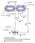
fig6.gif

Looking Forward to hearing from you.
 

I usually use this site to download the 3D part design and then do it based on the footprint datasheet.
https://www.3dcontentcentral.com/Search.aspx?arg=PFF

- - - Updated - - -

if you you place the pads from one side of the story will be in another oval. Usually companies that make printed circuit boards identify it as being boring to spend the cutter and do it correctly.
 

here is something very similar. it is a good starting point.
 

Attachments

  • XDCR_ACS754LCB(18-Sep-2012 07-27).zip
    9.5 KB · Views: 127
but actually as you can see in the picture attched there is missing information about the radius of the through hole pad ,
What do you think about this problem?
Can you give me some idea about how i can draw the pad???

- - - Updated - - -

I want to ask is the ACS758 will have the same radius of pad as the one you attched for ACS754?
 

As far as I can see all dimensions are present? could you highlight the one that you think isn't
 

The pad you are talking about I think is bigger pad (oblong pad)

Its dimensions are

Length: 0.039x2 + 0.157
width : 0.039
 

Yep I thought it might be, though I think you will find the width is actually 0.078 (1.95mm) as 0.039 is the radius. The component legs are 1.50mm (+/- 0.10) as per the data sheet (search google for ACS758xCB, first hit should be data sheet).
The only thing that is missing is the metric dimensions for R1 and R2.
 

here is something very similar. it is a good starting point.

Thanks Bro, after checking the datasheets for ACS754LxCB and ACS758xCB and comparing the PCB Layout Reference View for both, It seems that the footprint you send for ACS754LxCB is same as the one I want for ACS758xCB.

Thanks for your help.
I really appreciate that.

Your Sis Hanooda
 
Status
Not open for further replies.

Part and Inventory Search

Welcome to EDABoard.com

Sponsor

Back
Top