Continue to Site

Welcome to EDAboard.com

Welcome to our site! EDAboard.com is an international Electronics Discussion Forum focused on EDA software, circuits, schematics, books, theory, papers, asic, pld, 8051, DSP, Network, RF, Analog Design, PCB, Service Manuals... and a whole lot more! To participate you need to register. Registration is free. Click here to register now.

Suitable CMOS process for 5GHz digital clock

Status
Not open for further replies.

viperpaki007

Full Member level 5
Joined
Jul 2, 2008
Messages
270
Helped
11
Reputation
22
Reaction score
8
Trophy points
1,298
Location
Finland
Activity points
3,395
Hi,

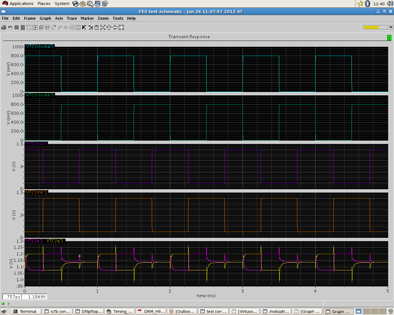
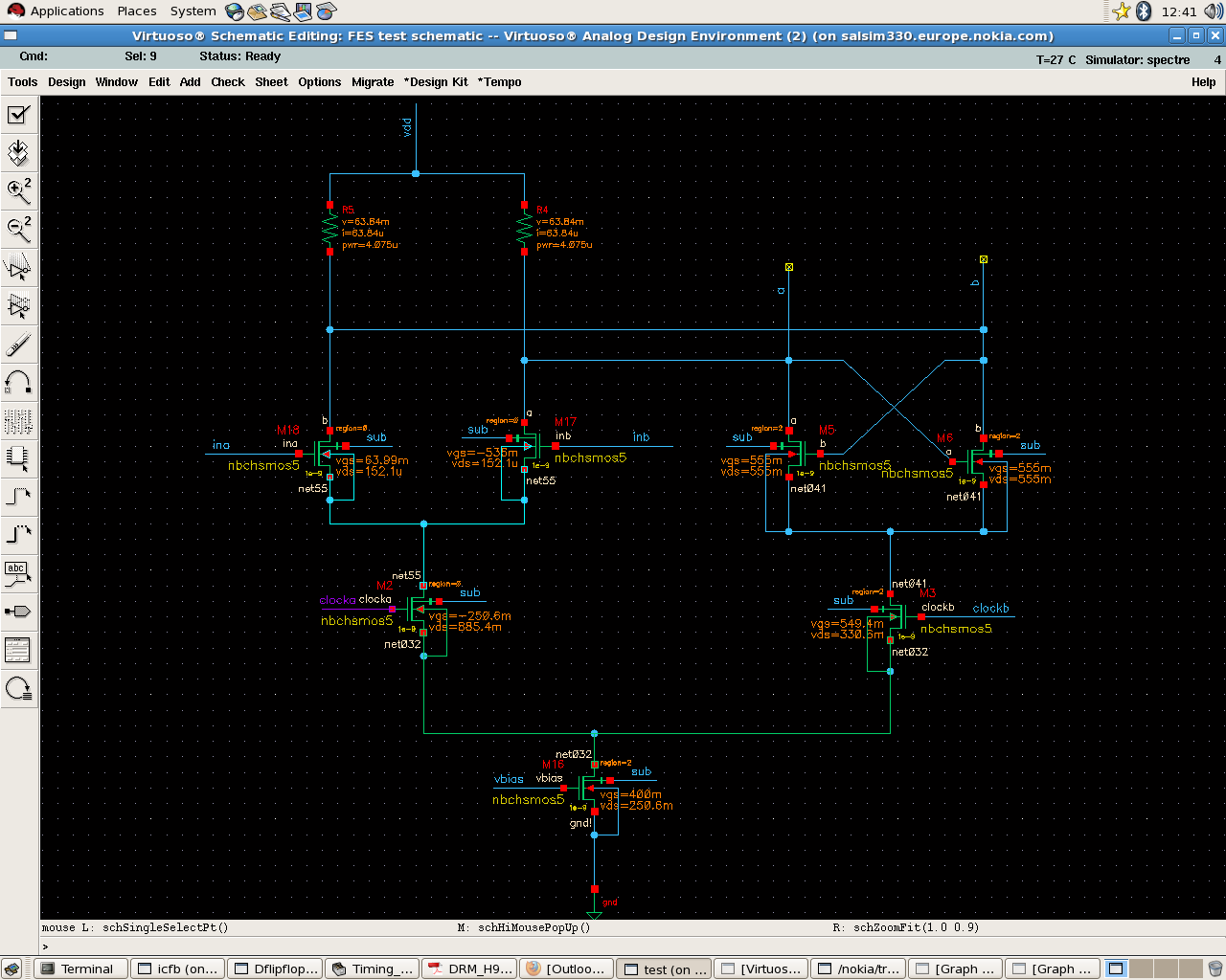
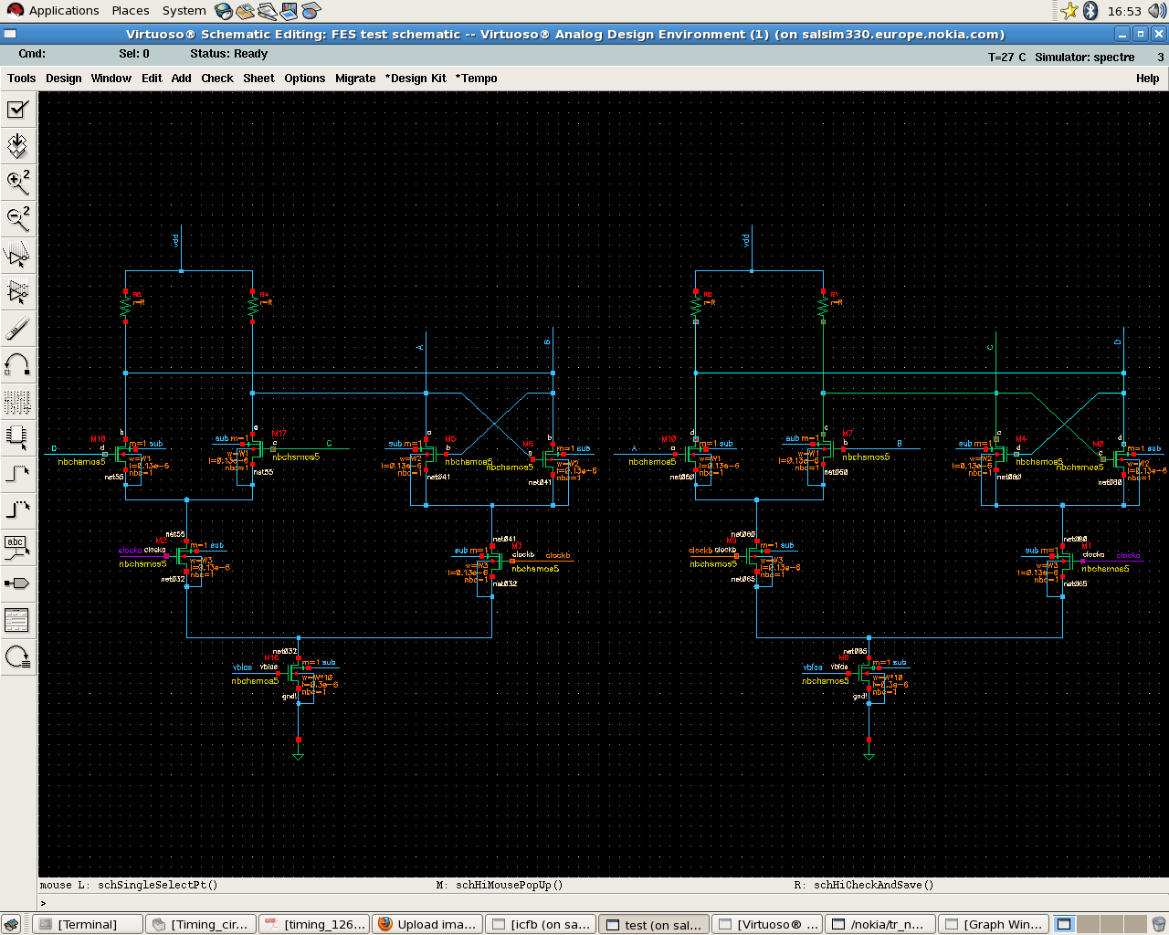
I need to use 5GHz digital clock for my timing circuit. At the moment, i am using 130nm CMOS and it stops working above 1.5GHz clock because of long propagation delays. Can anybody tell which CMOS process i should use to use for digital clock up-to 5GHz. Moreover, what kind of transistor lengths and widths i should use (At the moment i am using minimum lengths and widths).
 

It is likely that you need to go to a low-swing, differential
clock and compatible logic. Bang-bang CMOS logic is unlikely
to settle in one half-cycle with any wireload at all, not to
mention gate load.
 

I am afraid i am unable to get what you meant. Can you please elaborate your comments. I am a beginner in digital CMOS design.

Moreover, i can also explain my circuit a little bit. I am using Transmission gate flip-flops to divide the clock frequency by 2. Then I am generating 25% clock using the same flip-flops. Is there some kind of problem in my design which is preventing me to go for higher frequencies?
 

You might have to use a CML divider to divide a sinewave (or square-like sinewave) as much as you like, and then buffer it to CMOS levels.

WATER_10470_2010_9452_Fig15_HTML.jpg


You should also check if you can use TSPC freq divider. It is faster than simple CMOS but I don't know if it can reach 5GHz.
 
Hi Iamoun.

Thanks for the help. I searched for CML based D-flipflop on internet but so far haven't been able to get any good tutorial. Can you provide any link. Moreover, If i use CMOS buffer at output of CML divider (for logic level shifting), Will the buffer itself not slow down the circuit speed. In addition, how should i generate CLK_pos and CLK_neg signals for this high speed design. Previously i have been using the circuit in the following link for non overlapping clock generation..but it is quite slow

https://tams-www.informatik.uni-ham...12-gatedelay/40-tpcg/two-phase-clock-gen.html
 

First you should design a CML-to-CMOS converter (could be a simple single-ended differential pair) and use it as a load when you design the CML latches.
Anyway the converter will probably have low input capacitance. Fig.3.5 of the last link should give you the insight you need.


--- Who would provide you the 5GHz CMOS clock in the first place??
The differential clock signal will probably be provided by another circuit, such as a VCO. But you should just use a couple of sin sources.


Here is a little bit about CML dividers and CML latches.

**broken link removed**

**broken link removed** (Ch.3)
 
Hi,

I only have a 0 to 2.5V 5GHz clock from external source and its not differential. How should i generate non-overlapping CMOS logic from it and then use this non-overlapping clock to make differential CML signals.

Moreover, How the output of CML divider will be converted back to CMOS logic
 
Last edited:

You might begin with the simplest case, an inverter taper chain.
Say 1:4 as a good case. If you see edges getting sharper as you
move down the chain then CMOS logic is capable. If edges get
softer and you see a sinusoidal signal that never hits the rail,
you can forget doing anything useful in standard CMOS style.

Use a capacitor-blocked, self-biased inverter for your input
stage with a couple of 1:1 stages behind it for initial squaring.

A dynamic DFF could work for simple division and logically
combining this with the input clock could give you a 4-phase
clock field (with a lot of quality-dependence on input signal
symmetry, etc.). You might however find that phase sequence
is not entirely deterministic without some sort of reset, whose
baggage will slow the logic even more.
 
  • Like
Reactions: lamoun

    lamoun

    Points: 2
    Helpful Answer Positive Rating
If you follow dick_freebird's advice and find out your process can't handle this speeds, then an easy way to convert the 5GHz signal to differential clock would be to use a resistor loaded differential pair with CMOS clock at one input and suitable DC voltage at the other one.

PS. You won't need a non-overlapping clock with CML divider.
 

Hi Lamoun,

Do you mean that i should give a DC voltage at CLK_neg input of circuit in Figure 3.1 of following thesis

**broken link removed**


and one of my other main concerns is still unclear. How i will convert the CML logic back to CMOS logic later on?
 

Do you mean that i should give a DC voltage at CLK_neg input of circuit in Figure 3.1 of following thesis

Use a simple diff pair like that, and give a DC voltage to one input and CLK to the other.

The+MOSFET+differential+pair+for+the+purpose+of+deriving+the+transfer+characteristics%252C+iD1+and+iD1+versus+vid%253DvG1+-vG2.JPG


and one of my other main concerns is still unclear. How i will convert the CML logic back to CMOS logic later on?

You can use this circuit (It is not necessary to use the feedback resistor)

WATER_211972_1_En_4_Fig7_HTML.jpg
 
Hi Iamoun,

Can you suggest what will be the input logic levels for the CML clock and input. I am having trouble in getting the right output during the simulations.
 

Unfortunate I can't give you specific numbers you will need to find that yourself running sims.
As a starting point you will need to have such a DC common voltage (for clock and input) so as not to force the current source into triode region.
The signal swing must be high enough to fully switch the current between the circuit branches.
 
Hi lamoun,

I tried to change the input logic levels of CML latch so that all transistors work in the saturation region. However, i am having some problems during the hold phase of latch. Output 'a' and 'b' should be differential to each other in hold phase but both of them are showing high logic for some reason. I am attaching the circuit diagram and simulation results with this thread.


Looking forward for your suggestions
 

Hello viperpaki007,

Try to increase the output swing (double the load resistors or double the current)
also for the clock don't use a 0-800mV swing, try a 400mV - 1200mV. (M2 and M3 work as switches)

If that doesn't do the trick, try changing the transistor sizes (for example make M17 and M18 2*times larger than M5,M6)

*Also keep in mind that the clock waveforms will probably be more sine-like than pulse-like
 
Hi lamoun,


Thank you for the help. After changing the clock levels and increasing R, now the circuit is operating much better. However, there are still glitches in the output and i am not sure how to remove them. More importantly, what kind of output should i get from this structure ideally?

I am attaching my simulation results of CML flipflop as divide by 2 circuit. looking forward for your suggestions.


The glitches are here to stay. You might be able to minimize them a bit (maybe try 0.5/0.6 - 1.2V clock, playing with transistor sizes) but in the end, after you buffer the signal, they will probably disappear.
 
Hi Iamoun,

Right now my clock is generated from ideal pulse sources. Is it possible that these ideal sources are causing the glitches? What if i put a buffer after the ideal pulse source to make the clock more real?
 

The fast rising/falling edges of the ideal sources can introduce glitches, you have nothing to loose trying. Also don't forget add the appropriate load to the divider, this will smooth the output a bit.
 

Status
Not open for further replies.

Part and Inventory Search

Welcome to EDABoard.com

Sponsor

Back
Top