mmitchell
Advanced Member level 4
Hi,
How does EM wave transmit in a PCB board?
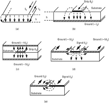
Assume that we have a two-terminal component of which one lead is connected to the ground plane (return path), and another to a receiver through a PCB trace.
Could someone who really understands Maxwell equations and waveguide help with the question?
Matt
How does EM wave transmit in a PCB board?
Assume that we have a two-terminal component of which one lead is connected to the ground plane (return path), and another to a receiver through a PCB trace.
- If the lead of both the transmitter and the receiver are on the outer layer of the PCB board so that they are directly exposed to air (assume no solder mask coating), would the EM filed transmit to all directions into the air? After all, this is the solution of Maxwell’s equation in vacuum.
- If the EM wave does go to all-directions, then why do we still use a stripline (microstrip, etc.) to guide it?
- If the transmission line (stipline) is embedded in an inner layer of the board, how does the EM field actually travel? Is it confined to the PCB trace, or is confined to the FR4 dielectric, or could transmit to all directions in the air?
- I think it looks likely that the majority of EM wave would not transmit to air due to total reflection between FR4 and air boundary. FR4 has εr of 4, so that the incident angle which could cause total reflection is sin-1(1/4) = 14.47°. Therefore, it might be that only a small fraction of EM energy could FR4-air boundary, either at horizontal edges or from top/bottom layers, to air.
- If there the trace is sandwiched by power and ground planes, then due to reflection, no EM wave could penetrate enclosing power/ground layers, so that EM wave only travels in FR4 region enclosed by copper power/ground planes.
- Combining (a)(b): which is the actual reason preventing EM wave from radiating into air on a PCB board?
- However, normally (not considering things like buried resistors) all components are mounted on top/bottom layers, and if assuming no coating then they are directly exposed to the air. For such case FR4-air boundary cannot cause any total reflection to confine signal, and the only reason I could thought of is that EM waves are traveled totally in conductors themselves, not even in FR4. However, most of the calculation in signal propagation time seem to use v=c/sqrt(εr). I am confused which speed should I choose for external conductors (without coating).
Could someone who really understands Maxwell equations and waveguide help with the question?
Matt