According to my previous experience,
wideband matching from 700 MHz to 2700 MHz (GSM/WCDMA/LTE) can be achieved by mere 3 components.
If the frequency range is 2.4, 2.1, 1.8, 1.6, 0.9 GHz,
and you have 5 components,
just do the wideband matching from 0.9 GHz to 2.4 GHz
To start with, you need Smith Chart software, ADS or AWR is better.
Step1.
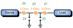
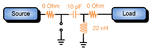
Remove all the shunt components,
and put 0 Ohm resistors in all the series location.
The aim is to know your original impedance.

Watch out!
You MUST NOT use solder bridge instead of 0 Ohm resistors. Because solder bridge has parasitic effect,
which impacts your original impedance.
Even if the same board,
with solder bridge in series location, different people have different measured original impedance.
Original impedance is the reference, your next steps are all based on it, if it’s not correct, your next steps are all in vain.
Step2.
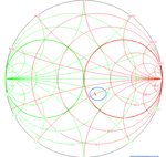
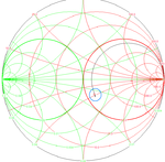
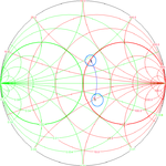
Let’s assume its PCB original impedance is [61.2-23.167j] Ohm,

and our next step is to make the impedance location move to the green and red circules with bold line shown as above.
Because these 2 circles pass through the 50 Ohm point. T
hat is to say, as long as you make your impedance location move to these 2 circles,
and then by means of following methods :

you can achieve 50 Ohm point.
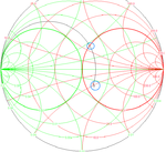
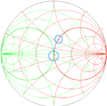
The first component we wanna determine its value is Z1.

Z1 is capacitor :

Z1 is inductor :

As shown above, for Z1, neither of C/L can make the impedance location move to the green and red circules with bold line.
In other words, Z1 can’t help us achieve 50 Ohm point.
Thus, we just make Z1 remain 0 Ohm resistor.
Step3.
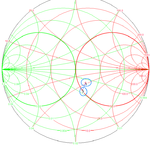
And, determine Z2 value
Z2 = 22 nH inductor

Z2 = 1pF capacitor

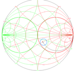
As shown above, for Z2, both C and L can make impedance location move to the green and red circules with bold line.
However, to shunt C may attenuate RF signal.
Let’s check :

As shown above, to shunt a 1pF capacitor has 0.75 dB insertion loss @ 2400 MHz.
Consequently, we choose Z2 = 22 nH inductor instead of 1pF capacitor.
Now, the impedance becomes [50 + 31j] Ohm

Step4.
And, determine Z3 value
Z3 = 10 pF

We find that the impedance becomes [50-0.833j] Ohm
It is already acceptable.
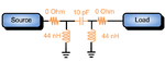
Therefore, now, your matching components are as below :

It’s just a L type form.
Step5.
The previous steps are based on one single frequency.
But, what you wanna do is the wideband matching from 0.9 GHz to 2.4 GHz.
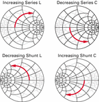
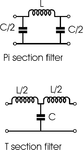
Thus, you need to shrink the impedance circle on Smith Chart further by means of T or Pi type.


As shown above, you can transform the L type to pi type, as illustrated below :

Generally speaking, you can begin to do the wideband matching with these 5 steps.
However, these steps are just beginning.
Because there is parasitic effect in your PCB layout trace and matching components.
Besides, both inductors and capacitors have SRF.
These factors make your impedance trace on the Smith Chart is not as what you expected
while doing the matching, even more than expected.
Consequently, you should begin to do the wideband matching with these 5 steps,
and tune the L/C value with measurement shown in VNA.
wideband matching from 700 MHz to 2700 MHz (GSM/WCDMA/LTE) can be achieved by mere 3 components.
If the frequency range is 2.4, 2.1, 1.8, 1.6, 0.9 GHz,
and you have 5 components,
just do the wideband matching from 0.9 GHz to 2.4 GHz
To start with, you need Smith Chart software, ADS or AWR is better.
Step1.
Remove all the shunt components,
and put 0 Ohm resistors in all the series location.
The aim is to know your original impedance.
Watch out!
You MUST NOT use solder bridge instead of 0 Ohm resistors. Because solder bridge has parasitic effect,
which impacts your original impedance.
Even if the same board,
with solder bridge in series location, different people have different measured original impedance.
Original impedance is the reference, your next steps are all based on it, if it’s not correct, your next steps are all in vain.
Step2.
Let’s assume its PCB original impedance is [61.2-23.167j] Ohm,
and our next step is to make the impedance location move to the green and red circules with bold line shown as above.
Because these 2 circles pass through the 50 Ohm point. T
hat is to say, as long as you make your impedance location move to these 2 circles,
and then by means of following methods :
you can achieve 50 Ohm point.
The first component we wanna determine its value is Z1.
Z1 is capacitor :
Z1 is inductor :
As shown above, for Z1, neither of C/L can make the impedance location move to the green and red circules with bold line.
In other words, Z1 can’t help us achieve 50 Ohm point.
Thus, we just make Z1 remain 0 Ohm resistor.
Step3.
And, determine Z2 value
Z2 = 22 nH inductor
Z2 = 1pF capacitor
As shown above, for Z2, both C and L can make impedance location move to the green and red circules with bold line.
However, to shunt C may attenuate RF signal.
Let’s check :
As shown above, to shunt a 1pF capacitor has 0.75 dB insertion loss @ 2400 MHz.
Consequently, we choose Z2 = 22 nH inductor instead of 1pF capacitor.
Now, the impedance becomes [50 + 31j] Ohm
Step4.
And, determine Z3 value
Z3 = 10 pF
We find that the impedance becomes [50-0.833j] Ohm
It is already acceptable.
Therefore, now, your matching components are as below :
It’s just a L type form.
Step5.
The previous steps are based on one single frequency.
But, what you wanna do is the wideband matching from 0.9 GHz to 2.4 GHz.
Thus, you need to shrink the impedance circle on Smith Chart further by means of T or Pi type.
As shown above, you can transform the L type to pi type, as illustrated below :
Generally speaking, you can begin to do the wideband matching with these 5 steps.
However, these steps are just beginning.
Because there is parasitic effect in your PCB layout trace and matching components.
Besides, both inductors and capacitors have SRF.
These factors make your impedance trace on the Smith Chart is not as what you expected
while doing the matching, even more than expected.
Consequently, you should begin to do the wideband matching with these 5 steps,
and tune the L/C value with measurement shown in VNA.