Welcome to our site! EDAboard.com is an international Electronics Discussion Forum focused on EDA software, circuits, schematics, books, theory, papers, asic, pld, 8051, DSP, Network, RF, Analog Design, PCB, Service Manuals... and a whole lot more! To participate you need to register. Registration is free. Click here to register now.
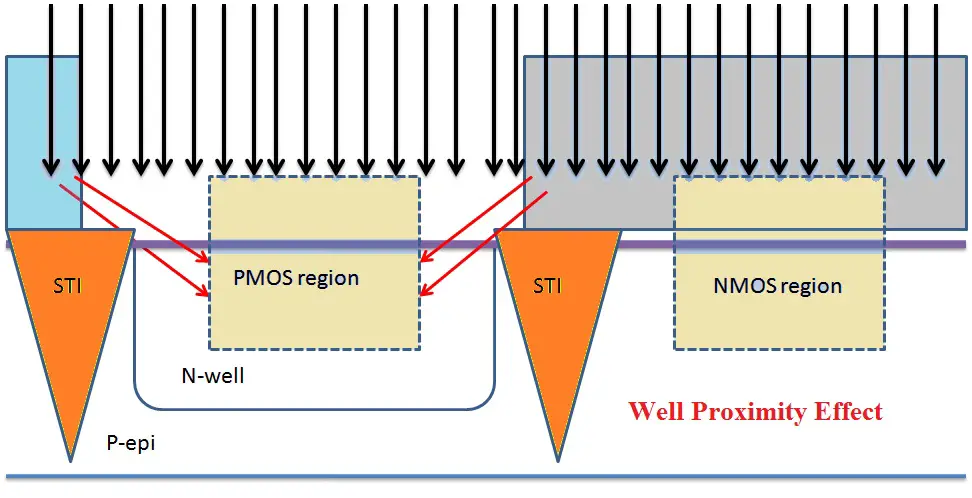
Well proximity effect (WPE) is due to lateral non-uniformity in well-doping and causes the MOSFET threshold voltages and other electrical characteristics to vary with the distance of the transistor to the well-edge.
siliconvlsi.com
Regards, Dana.
Attachments
Investigation of 65 nm CMOS transistor local variation -- Y.Z. Xu; C.S. Chen; J.T. Watt -...pdf
The additional capacitance (Cwpe) due to WPE can be modeled using a simple formula:Cwpe=εox⋅A⋅dwpe
where:
εox is the permittivity of the oxide,
A is the area of the well-channel overlap,
dwpe is the separation between the well and the channel.
This ratio of area/gap is true for all capacitance effects in PCB's and parasitics
Electric Field Distortion:
The electric field distortion (Edist) can be related to the change in voltage (Vgs) and the channel length (L)
:Edist∝Vgs/L
This is always how E fields are defined in [V/m] or [V/μm]
An increase in Edist contributes to a higher threshold voltage.
Threshold Voltage Shift:
The overall shift in threshold voltage (ΔVth) can be expressed as a combination of various factors:
ΔVth=Cwpe/Cox⋅(Vgs−Vth0)+Edist/Eox
where:
Cox is the oxide capacitance,
Vth0 is the threshold voltage without WPE,
Eox is the electric field due to the oxide.
Source/Drain (S/D) Orientation and Drain Current (Id):
Drain Current (Id) in Saturation:
The drain current in saturation (Idsat) can be expressed as:
Idsat=β/2⋅(Vgs−Vth−Vds/2)²
where:
β is the transconductance parameter. What about Ohmic region? Ids =β * (Vgs - Vth)²/2. when Vds~0 true/false?
Ohmic Region Behavior:
In the ohmic region, the drain current (Id) is approximately given by Ohm's Law:
Id=μ⋅Cox⋅W/L⋅(Vgs−Vth−Vds/2)
Transition from Ohmic to Saturation:
The transition from ohmic to saturation occurs when Vds≥Vgs−Vth. Beyond this point, the transistor enters the saturation region.
These formulas provide a quantitative understanding of how WPE affects threshold voltage (Vth) and how the drain current (Id) behaves in different regions. The actual values of parameters (β, μ, etc.) depend on the specific characteristics of the transistor and the technology used in its fabrication.
Comparing all diodes, FETs, and electrolytics, I have found a correlation in the product of R*C = Tau is constant for a given family or topology and geometry which also changes with Vmax rating. Using RdsOn, Coss or Ciss or ESR and C (0V) at some test temperature. The fundamental phenomena in physics is the ratio of C ∝Area/gap. In e-caps, capacitors with low ESR has to do with surface roughness (acid eteched) with a small gap.
Sorry, but still I didn't understand how Vth for NMOS is increasing. From my understanding, if during N-well implant if some Phosphorus atoms enter in P-sub(which is doped with Boron) so it will reduce the number of holes in PSUB which will lead to application of less VGS in order to create a n-channel.
This site uses cookies to help personalise content, tailor your experience and to keep you logged in if you register.
By continuing to use this site, you are consenting to our use of cookies.