Argoth
Newbie level 3
- Joined
- Jan 24, 2015
- Messages
- 3
- Helped
- 0
- Reputation
- 0
- Reaction score
- 0
- Trophy points
- 1
- Location
- Czech Republic
- Activity points
- 38
Hello,
I am trying realize wireless communication between two devices.
I have never done something like that and as a beginner I don't understand how some things work so I need your help.
I am using:
- Nexys 3 board with Spartan 6 FPGA
http://www.digilentinc.com/Products...5b85a628e-21AA2222-5056-0201-02D6A08418D6FF8E
- PmodRF2 transceiver
http://www.digilentinc.com/Products/Detail.cfm?NavPath=2,401,927&Prod=PMOD-RF2
On PmodRF2 there is microchip MRF24J40 that communicates with a host mictrocontroller via a 4 wire SPI port as a slave device. Microchip is an IEEE 802.15.4 Standard compliant 2.4 GHz RF transceiver and it integrate the PHY and MAC functionality.
So I guess I need write SPI master in FPGA something like... http://www.eewiki.net/display/LOGIC/Serial+Peripheral+Interface+(SPI)+Master+(VHDL)
And this I use for writing and reading data.
Now comes the part where I stopped. In MRF24J40 is implemented static RAM that looks like that.
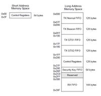
There are some control registers and I have no Idea how to use them. I know that there is some short and long address register interface. So could you please tell me how to use it. For example:
According to MRF24J40 manual I need initialize MRF24J40 like this:
1. SOFTRST (0x2A) = 0x07 – Perform a software Reset. The bits will be automatically cleared to ‘0’ by hardware.
2. PACON2 (0x18) = 0x98 – Initialize FIFOEN = 1 and TXONTS = 0x6.
3. TXSTBL (0x2E) = 0x95 – Initialize RFSTBL = 0x9.
4. RFCON0 (0x200) = 0x03 – Initialize RFOPT = 0x03.
5. RFCON1 (0x201) = 0x01 – Initialize VCOOPT = 0x02.
6. RFCON2 (0x202) = 0x80 – Enable PLL (PLLEN = 1).
7. RFCON6 (0x206) = 0x90 – Initialize TXFIL = 1 and 20MRECVR = 1.
8. RFCON7 (0x207) = 0x80 – Initialize SLPCLKSEL = 0x2 (100 kHz Internal oscillator).
9. RFCON8 (0x208) = 0x10 – Initialize RFVCO = 1.
10. SLPCON1 (0x220) = 0x21 – Initialize CLKOUTEN = 1 and SLPCLKDIV = 0x01.
I think that I should move register on adress 0x2A to adress 0x07. Is it right? And if yes, how?
And another thing for example with channel selection. There is some RFCON0 (0x200) register. I choose channel and according to this I should set value like ,,0x03,, into RFCON0 (0x200<7:4>). So it is value 0011 in bits 7 6 5 4 ? And how to do that?
The problem is that I dont know what to send through SPI and how it should looks like in VHDL.
Thanks for help
I am trying realize wireless communication between two devices.
I have never done something like that and as a beginner I don't understand how some things work so I need your help.
I am using:
- Nexys 3 board with Spartan 6 FPGA
http://www.digilentinc.com/Products...5b85a628e-21AA2222-5056-0201-02D6A08418D6FF8E
- PmodRF2 transceiver
http://www.digilentinc.com/Products/Detail.cfm?NavPath=2,401,927&Prod=PMOD-RF2
On PmodRF2 there is microchip MRF24J40 that communicates with a host mictrocontroller via a 4 wire SPI port as a slave device. Microchip is an IEEE 802.15.4 Standard compliant 2.4 GHz RF transceiver and it integrate the PHY and MAC functionality.
So I guess I need write SPI master in FPGA something like... http://www.eewiki.net/display/LOGIC/Serial+Peripheral+Interface+(SPI)+Master+(VHDL)
And this I use for writing and reading data.
Now comes the part where I stopped. In MRF24J40 is implemented static RAM that looks like that.
There are some control registers and I have no Idea how to use them. I know that there is some short and long address register interface. So could you please tell me how to use it. For example:
According to MRF24J40 manual I need initialize MRF24J40 like this:
1. SOFTRST (0x2A) = 0x07 – Perform a software Reset. The bits will be automatically cleared to ‘0’ by hardware.
2. PACON2 (0x18) = 0x98 – Initialize FIFOEN = 1 and TXONTS = 0x6.
3. TXSTBL (0x2E) = 0x95 – Initialize RFSTBL = 0x9.
4. RFCON0 (0x200) = 0x03 – Initialize RFOPT = 0x03.
5. RFCON1 (0x201) = 0x01 – Initialize VCOOPT = 0x02.
6. RFCON2 (0x202) = 0x80 – Enable PLL (PLLEN = 1).
7. RFCON6 (0x206) = 0x90 – Initialize TXFIL = 1 and 20MRECVR = 1.
8. RFCON7 (0x207) = 0x80 – Initialize SLPCLKSEL = 0x2 (100 kHz Internal oscillator).
9. RFCON8 (0x208) = 0x10 – Initialize RFVCO = 1.
10. SLPCON1 (0x220) = 0x21 – Initialize CLKOUTEN = 1 and SLPCLKDIV = 0x01.
I think that I should move register on adress 0x2A to adress 0x07. Is it right? And if yes, how?
And another thing for example with channel selection. There is some RFCON0 (0x200) register. I choose channel and according to this I should set value like ,,0x03,, into RFCON0 (0x200<7:4>). So it is value 0011 in bits 7 6 5 4 ? And how to do that?
The problem is that I dont know what to send through SPI and how it should looks like in VHDL.
Thanks for help