Continue to Site

Welcome to EDAboard.com

Welcome to our site! EDAboard.com is an international Electronics Discussion Forum focused on EDA software, circuits, schematics, books, theory, papers, asic, pld, 8051, DSP, Network, RF, Analog Design, PCB, Service Manuals... and a whole lot more! To participate you need to register. Registration is free. Click here to register now.

Why do they put solder on some tracks in power mains supplies?

Status
Not open for further replies.

userx2

Full Member level 3
Joined
Sep 19, 2008
Messages
168
Helped
2
Reputation
4
Reaction score
3
Trophy points
1,298
Activity points
3,022
Maybe this is another stupid question but here it goes:

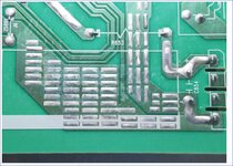
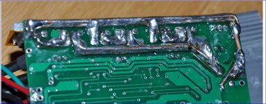
A lot of PCB tracks in power supplies have a strip of exposed solder running on top of them.

I once thought this is to increase the current capacity of a track but when I looked into that, it appears that solder does not really do much for the current capacity.
Or is it done for allowing test fixtures to make contact during production testing?
I really do not know.
Solder on PCB tracks.JPG

So what is the real reason?


Regards
X
 

Hi
Dont say it's stupid question we all learn 🤗
For sure it about current handeling capacity
Lock at it
All the add solder is at power track.
 

Absolutely for increasing current capacity. Solder may not be quite as good as copper but making a PCB with say 0.5mm thick copper would be prohibitively expensive. Simply leaving the resist layer off power tracks and letting the wave soldering process thicken the tracks is far far cheaper and almost as effective.

Brian.
 

Hi,

I´d say it´s a myth that adding solder can significantly increase current capability.

Now what is "significantly"? 50% more current? twice the current (100% more)? 3 times? even more?

The shown PCB looks like a cheap product from the 1980ies. At this time they mainly used solder with about 35% Pb.
This solder has about 10% (9..13%) the conductance of copper.
So if you want to reduce the resistanc to - let´s say - half of the initial value than your solder (including Cu) needs to be about 10 times the copper thickness. So from 35um to 350um. And it needs to be as uniform as possible, because the parts with lower thickness will have the highest impact on overall resistance.

On the shown picture the effective solder thickness is less than 350um. And - even worse - it´s not uniform across all over the copper trace width. It rather seems to cover maybe 70% of the width.
So I expect the resulting resistance maybe is 60-70% of the initial value. Or 140 - 160% of increase in conductivity.

But this does not mean you can run 140..160% of the current, because P ~ I * I
so yu have to take the sqaure root. The increase in current capability is 20..25%.

***
Out of curiosity I did an experiment.
I had an old PCB with a 35mm long, 1.27mm wide, 35um thick trace.
Math said it should be about 14.5 mOhms.

I measured (all very accurate with 4 wire and at identical temperature) 13.4 mOhms
(This is less than expected. Maybe because of my messurement errors in length and width. .. or a bit higher copper plating)

Then I added solder over the whole width with "usual" thickness. Maybe 0.2mm effective:
Result: 10.8 mOhms (identical to increase in width from 1.27mm to 1.57mm .. just 0.30mm)

Then I spend some time to put some ugly thick solder on it. It really was hard to do this. And it looked awful. I guess there were parts with 1mm thickness (mind the usual PCB thickness is 1.6mm) other parts maybe had down to 0.5mm.
The result was about 7mOhms.

Again:
Initial: 13.4 mOhms, 100% current
normal: 10.8 mOhms, 111% current (11.3% increase)
ugly: 7mOhms, 138% current, (38.3% increase)

--> I see no way to reliably increase current capability to let´s say 150% by adding solder.
***

Not tested the increase in thermal dissipation.
It´s known that the solder stop increases thermal resistance. So omitting it will decrease the temperature rise.
But this is independent of the "added solder".


Klaus
 
Just a stray thought, but solder also increases the thermal
mass substantially and if you are dealing with a pulsed
current, maybe "smooths" the temperature excursions
where thin copper alone, might respond more "real time"
with thermal spiking, trace delamination, etc.?

But the solder might still just be a blind stab at "better,
cheaply".
 

Hi,

I´d say it´s a myth that adding solder can significantly increase current capability.

Now what is "significantly"? 50% more current? twice the current (100% more)? 3 times? even more?

The shown PCB looks like a cheap product from the 1980ies. At this time they mainly used solder with about 35% Pb.
This solder has about 10% (9..13%) the conductance of copper.
So if you want to reduce the resistanc to - let´s say - half of the initial value than your solder (including Cu) needs to be about 10 times the copper thickness. So from 35um to 350um. And it needs to be as uniform as possible, because the parts with lower thickness will have the highest impact on overall resistance.

On the shown picture the effective solder thickness is less than 350um. And - even worse - it´s not uniform across all over the copper trace width. It rather seems to cover maybe 70% of the width.
So I expect the resulting resistance maybe is 60-70% of the initial value. Or 140 - 160% of increase in conductivity.

But this does not mean you can run 140..160% of the current, because P ~ I * I
so yu have to take the sqaure root. The increase in current capability is 20..25%.

***
Out of curiosity I did an experiment.
I had an old PCB with a 35mm long, 1.27mm wide, 35um thick trace.
Math said it should be about 14.5 mOhms.

I measured (all very accurate with 4 wire and at identical temperature) 13.4 mOhms
(This is less than expected. Maybe because of my messurement errors in length and width. .. or a bit higher copper plating)

Then I added solder over the whole width with "usual" thickness. Maybe 0.2mm effective:
Result: 10.8 mOhms (identical to increase in width from 1.27mm to 1.57mm .. just 0.30mm)

Then I spend some time to put some ugly thick solder on it. It really was hard to do this. And it looked awful. I guess there were parts with 1mm thickness (mind the usual PCB thickness is 1.6mm) other parts maybe had down to 0.5mm.
The result was about 7mOhms.

Again:
Initial: 13.4 mOhms, 100% current
normal: 10.8 mOhms, 111% current (11.3% increase)
ugly: 7mOhms, 138% current, (38.3% increase)

--> I see no way to reliably increase current capability to let´s say 150% by adding solder.
***

Not tested the increase in thermal dissipation.
It´s known that the solder stop increases thermal resistance. So omitting it will decrease the temperature rise.
But this is independent of the "added solder".


Klaus
Thank you Klaus for that detail.

The PCB I showed is actually less than 1 year old and is a motor controller for a milling machine auto feed.

I personally have actually done this once on a PCB track where I thought it will help.
There is however no way of telling and I have never seen any calculations or detailed explanations on how to work out the increase in capacity.
I then stumbled across some paper that said it was basically futile, as you also said.

In some old school, or "real" stuff, I have seen copper wire or strips soldered onto tracks instead of just solder. That makes much more sense.

And how does it work in the case of the attached picture? The solder is applied in a pattern and for some reason it does not go to one the pads on a track.

I also attached a picture of a PCB where copper has been added, just for comparison.
 

Attachments

  • Solder on tracks2.JPG
    Solder on tracks2.JPG
    125.5 KB · Views: 146
  • Solder and wire on tracks3.JPG
    Solder and wire on tracks3.JPG
    81.8 KB · Views: 109

resistivity of copper = 0.0177 E-6 ohm.meter

solder = 0.171 E-6 ohm.meter, for 60/40 solder

so a difference of just under 9.7 x

1 Oz copper is 35um thick, so to halve the R the solder needs to be 388um = 0.34 mm thick

to take the R to one quarter the solder will need to be 1mm thick

there may well be some short term thermal benefit.
--- Updated ---

@betwixt, re: "Simply leaving the resist layer off power tracks and letting the wave soldering process thicken the tracks is far far cheaper and almost as effective."

Solder isn't all that cheap if you are leaving behind 1-2mm on a lot of tracks ....
 

It does look like a cheap attempt to increase the current carrying capacity of the trace (rather than redoing the board to increase the trace widths).
I have soldered a coper wire onto a trace to reduce its resistance (for a sensitive A/D converter application), but that's obviously a time-consuming, expensive process.
 

Status
Not open for further replies.

Similar threads

Part and Inventory Search

Welcome to EDABoard.com

Sponsor

Back
Top