Continue to Site

Welcome to EDAboard.com

Welcome to our site! EDAboard.com is an international Electronics Discussion Forum focused on EDA software, circuits, schematics, books, theory, papers, asic, pld, 8051, DSP, Network, RF, Analog Design, PCB, Service Manuals... and a whole lot more! To participate you need to register. Registration is free. Click here to register now.

Which layout configuration?

Status
Not open for further replies.

AMSA84

Advanced Member level 2
Joined
Aug 24, 2010
Messages
577
Helped
8
Reputation
16
Reaction score
8
Trophy points
1,298
Location
Iberian Peninsula
Activity points
6,178
Hi guys, I would like to ask you for you opinion.

I am designing a simple current mirror, and I'd like to know which way is best to interleave the transistors:

1 - 25/1.5um
2 - 250/1.5um

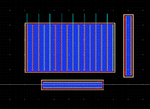
In the left side you can see a configuration of 22 transistors - 20 for the 250/1.5um (which gives 12,5um per finger) and 2 x 12,5um (for the 25um transistor).

The idea was to get this config:

AAAAAAAAAA BB AAAAAAAAAA

The starting diffusion is the source so that in the transition A to B they share the source.

On the right configuration, you can see:

12 transistors - 10 for the 250/1.5um (which gives 25 per finger) and the 1 + 1 of 25um each one. In this configuration I have to add a "dummy" transistor in order to get the perfect match between the diffusion.

Which one should I go for?

In one case I have long channel length on the other not, which might translate in more parasitic capacitance and resistance when compared to the other option?

Regards. which one.png
 

I would choose the one on the right since it is more square than the other. If it is square you avoid having to much effect from a gradient due to a long dimension.

Note that in both channel length is the same, it is the width that changes and the gate resistance. If the current mirror is only for biasing you should not worry too much about parasitics unless you are turning on/off the block frequently, or there is a fast moving signal going through the block.
 

Thanks for the reply.

What I wanted to say is that the width of the second one is higher than the other.

Well, this is to bias a comparator block that will have a very fast signal. In this case whats your opinion?
 

I would still prefer the right one.

Two things:
1) in the right case the capacitance should be less. The capacitance due to the area is the same but you have less perimeter in total, so less sidewall capacitance.

2) It depends what comparator topology you have, but if the current mirror is an active load, then total capacitance should be a factor. If the current mirror is to provide a tail current, you only need to worry about the drain capacitance on the output side of the mirror.

In addition, as you can see the layout on the right also keeps the routing minimal which helps minimize parasitics even further.
 
  • Like
Reactions: AMSA84

    AMSA84

    Points: 2
    Helpful Answer Positive Rating
Hi. Okay, thanks.

The current mirror is to bias the comparator. The comparator topology is that one based on the 3-current mirror (symmetrical OTA) with crosscouple load, to get positive feedback.

Regards.
 

By the way. Another question:

Which distance one should have between the guard rings and the components?
 

I would choose the left one because of the speed. It will be quicker in this case (one side gate contact). Poly has higher resistance so RC would be worse with wider transistor.
And question distance: it depends on choosen technology. There might be a Nwell proximity effect. And it also depends what type of component you want to place there (noisy, power hungry ...).
 

I will prefer the left one. With more drain fingers it will support more currents. But again it will be case by case basis.
 

Thanks for the reply guys.

Allow me to ask you another thing:

In the current mirror I know that the best thing to do is to interdigitate the transistors. However, I am facing this problem: If I want to inter-digitize the current mirror transistor 20/1.5um with a 230/1.5um transistor I could do 2 things:

1st - Make 2 x 10um and 23 x 230um then make BAAAAAAAAAAAAAAAAAAAAAAAB or AAAAAAAAAAAABBAAAAAAAAAAA. Don't know if it make sense, because it would give a giant configuration.
2nd - keep both separated and then here I could do 2 things (image bellow):

current.png

Now the question is which way I could put the "single" transistor. I know that one should adopt the all transistor in same orientation but in this case it is more convinient to put him horizontally (the single) and the other in the vertical.

What you guys can suggest?

EDIT: By the way, can I short the gates on both sides or it is not recommended? (more parasitic capacitances, right?)
My tech is UMC130nm.

Another questions, how many contacts (length) should I use in the guard ring? 1, 2 or 3?
 
Last edited:

Thanks for the reply guys.

Allow me to ask you another thing:

In the current mirror I know that the best thing to do is to interdigitate the transistors. However, I am facing this problem: If I want to inter-digitize the current mirror transistor 20/1.5um with a 230/1.5um transistor I could do 2 things:

1st - Make 2 x 10um and 23 x 230um then make BAAAAAAAAAAAAAAAAAAAAAAAB or AAAAAAAAAAAABBAAAAAAAAAAA. Don't know if it make sense, because it would give a giant configuration.
2nd - keep both separated and then here I could do 2 things (image bellow):

By the way why do you want keep that just in one column/row? You can make cross-quad.

Now the question is which way I could put the "single" transistor. I know that one should adopt the all transistor in same orientation but in this case it is more convinient to put him horizontally (the single) and the other in the vertical.

What you guys can suggest?

Do you want to match that single transistor with the rest? Because it cannot be matched properly and you can affect already matched structure in negative way.
If it would be my call I would put him vertical and split him into two fingers.

EDIT: By the way, can I short the gates on both sides or it is not recommended? (more parasitic capacitances, right?)
My tech is UMC130nm.

I usually contact each side of gate poly if transistors width is significant. And this is that case. But if I want to keep parasitic cap small as possible only one contacted side is enough. But it's trade off between parasitic cap and speed.

Another questions, how many contacts (length) should I use in the guard ring? 1, 2 or 3?

It depends on leakage. Is it high enough to shift substrate to not desired voltage? If not put there just one.
 

Thanks for the reply jirika.

Regading the cross-quad, you mean doing common centroid? Well, I imagine that doing that crossquad would increase the parasitics, which is crucial because this comparator is to operate at very high frequency.
 

Status
Not open for further replies.

Part and Inventory Search

Welcome to EDABoard.com

Sponsor

Back
Top