Continue to Site

Welcome to EDAboard.com

Welcome to our site! EDAboard.com is an international Electronics Discussion Forum focused on EDA software, circuits, schematics, books, theory, papers, asic, pld, 8051, DSP, Network, RF, Analog Design, PCB, Service Manuals... and a whole lot more! To participate you need to register. Registration is free. Click here to register now.

Post-layout Results are not correct

hosseineslahi7

Junior Member level 1
Joined
Apr 4, 2018
Messages
19
Helped
0
Reputation
0
Reaction score
0
Trophy points
1
Activity points
246
Dear experts,
I have designed a simple design working as a level-shifter and buffer at 1GHz in GF22nm technology. Then, my colleague and I designed two roughly similar layouts for my design, however, we see completely different post-layout results. We carefully connected the back-gates, DEEP NWELL layers, substrate, gnd and VDD to the correct biases on both layouts. The floorplans are also similar with minor changes in the wiring routs only. So, we could not understand what is going on.

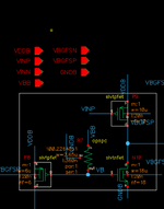
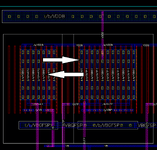
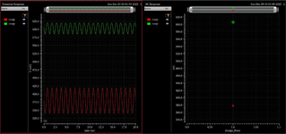
Then I realized that if I change the location of only two PMOS devices (P9 and P8 on schematic) in my layout, as I showed in figures 1 and Figure 2, posy-layout results will change dramatically. You can see the difference in figure 3. It means a small change in layout will shift the result.

Does anyone know how it is possible? Is it because of my design or something is wrong in PDK?
 

Attachments

  • Figure1.png
    Figure1.png
    50.9 KB · Views: 86
  • Figure2.png
    Figure2.png
    158.3 KB · Views: 81
  • Figure3.png
    Figure3.png
    1.3 MB · Views: 92
Perhaps is it a proximity coupling effect, why don't you run the
two analog extracted netlists side by side and see what you can see?
 
if it's layout dependant effect then one by one switch off the WPE (well related) and STI (stress related) switches and observe the difference. IF they do not make a difference you should look very carefully at your layout.
 
if it's layout dependant effect then one by one switch off the WPE (well related) and STI (stress related) switches and observe the difference. IF they do not make a difference you should look very carefully at your layout.
Thanks for your response.
How can I control STI and WPE switches? I have not done that before?
--- Updated ---

Perhaps is it a proximity coupling effect, why don't you run the
two analog extracted netlists side by side and see what you can see?
Yes, It is a good idea. I had to run simulations with/without the floorplan parasitic effect and see what happens. It is not a logical method but I had to optimize the floorplan to find the best one for layout. I did it by using the Layout "(Parasitics/LDE)" option in ADE XL window. However, I saw weird post-layout results after wiring and I should meet this problem also.
 
Last edited:
well if its calibre LVS for PEX a form appears and maybe the same for PVS for PEX and you'll see WPE and STI options on a list of things that can be set during LVS because for obvious reasons this is where the well and STI dimensions are extracted for use in the bsim model. This also requires an additional license to use. If you cannot see these I'll take a screen shot and post to help you identify what to look for.

I have also fould that if you accidentally leave some unused or wrong layer it might extract properly but simulate wrong. Once I left a np layer square soemwhere and it messed up the simulation. Daft careless mistake I made I know but sometimes these thing happen!
 

LaTeX Commands Quick-Menu:

Part and Inventory Search

Welcome to EDABoard.com

Sponsor

Back
Top