Continue to Site

Welcome to EDAboard.com

Welcome to our site! EDAboard.com is an international Electronics Discussion Forum focused on EDA software, circuits, schematics, books, theory, papers, asic, pld, 8051, DSP, Network, RF, Analog Design, PCB, Service Manuals... and a whole lot more! To participate you need to register. Registration is free. Click here to register now.

What's wrong with this LM350T circuit ? ( IC blown when shorted output )

Pigi_102

Member level 2
Joined
Nov 14, 2007
Messages
46
Helped
0
Reputation
0
Reaction score
0
Trophy points
1,286
Activity points
1,721
Hello all,
I've found a nice circuit around, for an LM350T variable power supply, and I built it.
Here the link:
https://www.eleccircuit.com/lm350-adjustable-voltage-regulator/
I added a second pot, as indicated in the linked page, for a precision settings, and thus the circuit become this one:
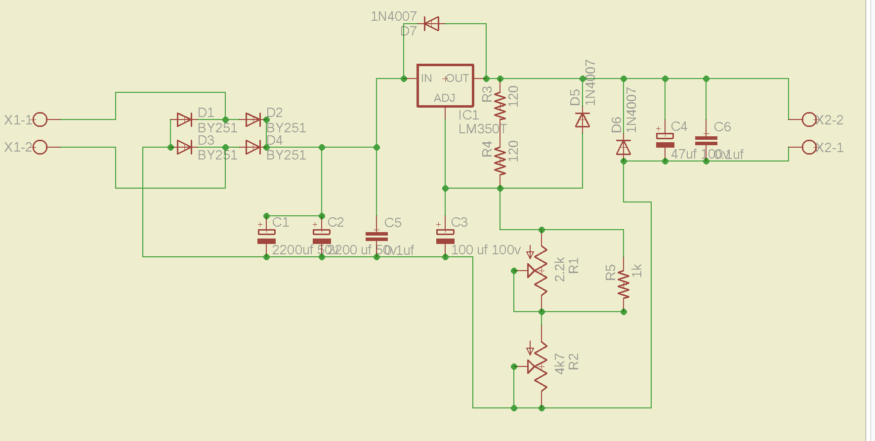
Schema_1.png


Everything was perfectly working ( voltage regulation and so on ) so basically I havn't made any (big ) mistake.
( In effect I did inverted values for C3 and C4 but it was working fine )

Reading trough the datasheet I've seen that the IC has short circuit protection so I tried to short the output ( I'm a bit disorded on my bench and sometimes it happen to me to have too much stuff on it and the output get shorted :D ) and immediatelly the LM350 blown.
Alle the diode were in correct position as per circuit and datasheet

Can someone help me in understanding why it blown ?

Thanks in advance

Pierluigi
 
X1-1 and X1-2 are the connection to the transformer. I have a 220V-16V ac transformer so the value is around that value ( 15V )

Pierluigi
 
What are symptoms of failure ?

When you turn off circuit and turn on again what voltages do you see ?

Others experience : https://www.eevblog.com/forum/beginners/output-short-circuit-keeps-killing-lm350t/

If you have a DSO you could capture the terminal V's when a short is applied, and see if any violation
occurs of its specs. Trigger DSO - going edge at some V, one shot capture. Might reveal other considerations, like excessive layout inductance.........

Show us a pic(s) of your prototype, its wiring, build, layout .....


Regards, Dana.
 
Last edited:
It might be a counterfeit part. There are many such "fake" parts in the market.
I recommend you to buy such parts form well known distributors.
 
It's hard to say, but I bought the IC from a local electronic store, not from ebay or amazon where it could more easily a counterfait part.

Symptoms of failure has been some sparc from output connector, when I shorted them, and then no more output from the circut. Also powering off and then on again, no more output.
I've "printed" a board ( I'm using eagle ) by using a presensibilized copper board and a bromograph so it's absolutelly in sync with the schema:
LM350_Board.png
and etched.
I've read the supplied link but no other components where blown. Only the LM350T.
My suspect is that the 100uf that was ( my mistake ) on the adj pin was way too high and sent a spike to the latter burning the IC.
I was wondering if someone can point out to a short circuit protection circuit that I could apply at the output ( or elsewhere ) to ( better ) protect the circut.
Could, eventually, this modification ( the TIP31 stuffs ) be usefull :
Schema_2.png


I'm not very good in electronic so I've copied here and there some solutions....

Pierluigi
 
X1-1 and X1-2 are the connection to the transformer. I have a 220V-16V ac transformer so the value is around that value ( 15V )

Pierluigi
Guessing? Knowing? Messured?
I expect something way different: about +/- 27V.

Did you read all the datasheet?
* external capacitors: They recommend disc or tantal - what did you use? They recommend 0.1uF or 1uF. Your values are much higher. And most probably much slower.
* what heatsink did yo use?
* Why the feedback (R3, R4) is 240 ohms, while the datasheet recommends 120 Ohms?
* Why did you use a TIP31 instead of 2N2222? High current vs low current. Slow vs fast?

****
* please keep on datasheet recommendations
* consdier to use a true solid GND plane on one layer of a 2 sided PCB.

Klaus
 
Hi Klaus.
Guessing? Knowing? Messured?
Measured. 16.5 V AC
Did you read all the datasheet?
Kind of. I followed the instruction on the link I posted in my first post. Then I've read it, but ...
* external capacitors: They recommend disc or tantal - what did you use? They recommend 0.1uF or 1uF. Your values are much higher. And most probably much slower.
Read before. Followed the web page.
* what heatsink did yo use?
A big heatsink but it was not heat at all. I wasn't drawing current until I shorted the output and IC blown in a millisecond
* Why the feedback (R3, R4) is 240 ohms, while the datasheet recommends 120 Ohms?
Again it was on the web page. The D/S instructs on 120 to 240 depending on applications. I'm not good to understand which is better and trusted the page.
* Why did you use a TIP31 instead of 2N2222? High current vs low current. Slow vs fast?
Again, I've found instruction on other pages, but TIP31 basically because of high wattage draw in case of short.

Pierluigi
.
 
Hi,
Measured. 16.5 V AC
Dana asked about "peak"..

Kind of. I followed the instruction on the link I posted in my first post. Then I've read it, but ...
My recommendation. Trust the datasheet. Who can know better than the manufacturer?
The manufacturer usually even provides applicationnnotes and more related informations.

Read before. Followed the web page.
No answer to my question. You rely on the "web page". Did you discuss your problem with them?
In my eyes they should take some responsibility for their informations.

A big heatsink but it was not heat at all. I wasn't drawing current until I shorted the output and IC blown in a millisecond
No heat .. but blown? I wonder: is this possible at all?
TIP31 basically because of high wattage draw in case of short.
Who said this? I ´d be interested in the physics and mathematics.

It´s the problem that everyone can post his "knowledge" in the internet. And often this knowledge isn´t much more than "I thought it would work" or "it worked for me" (in best case).

So my recommendation:
1) trust me ;-)
2) trust the datasheet
3) if my word is against the datasheet recommendation: trust the datasheet.


Klaus
 
Dana asked about "peak"..
Hard for me to see, but being a normal transformer I would even say 16.5 V
How can I measure a peak ( I don't have a DSO ) ? My tester says ( on AC ) 16.5V
No answer to my question.
You're right. Sorry. I've used polyester for 0.1uf ( and is wrong as per D/S ) I will change for ceramic ( If I've understood D/S ). All others are electrolityc.
Unfortunally D/S is way more generic, but I will try my best understanding to simplify schema as per D/S and try to get something more like the D/S.
TIP31 is because in case of short there could be a draw of 3A at 15 volts that could eventually lead to 5W while the transistor pull the ADJ to ground ( lowering the volt output ). Or I'm totally wrong ?
 
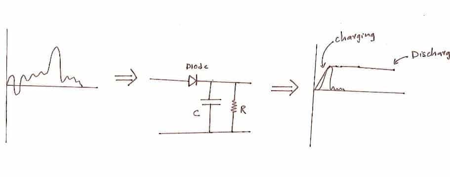
If you have a older analog scope you can see peak.

If you have no scope, and no other capability other than average reading DMM, you
could proto a quick peak detector on a breadboard. As simple as a diode and a CAP
will capture a "rough" peak measurement. For line low freq stuff.


You are correct in thought that an IC can be blown in ms, even uS. We used to delid parts
all the time finding static generated shorts and injection current shorts. They would
blow open bond wires and not leave any trace of heat. Failures can exhibit themselves in
various and fascinating ways. Some would melt silicon in hotspots, but average heat
miniscule. Others would look like they had been in a blast furnace. Most vendors
have/offer ap notes from their rel departments of failure modes, complete with pics and
SEM analysis screen shots......

Regards, Dana.
 
Last edited:
Hi,
Hard for me to see, but being a normal transformer I would even say 16.5 V
How can I measure a peak ( I don't have a DSO ) ? My tester says ( on AC ) 16.5V
When you have a transformer 220V / 16V..
* both values are RMS values
* both values are for full (resistive) load

So the realistic peak value is
* higher, because the line voltage varies and may become higher than 220V
* higher because of transformer production tolerance
* a lot higher on low load current (10 ... 20% higher than on full load)
* peak voltage of a perfect sine is V_RMS x SQRT(2) = V_RMS x 1.414

So a realistic/moderate value for me is (ignoring line voltage and production tolerance)
16V x 10% x 1.414 = 24.9V (positive as well as negative)
It also ignores noise and overshot caused by series inductance (ringing)

Unfortunally D/S is way more generic,
Is it? The datasheet usually tells you everything you need to know you need to know to operate the device correctly and stably.
Everything.
The manufacturer earns his money by selling it's devices. Thus they are interested in satisfied customers. Customers are satisfied when they get good assistance on technical problems and ... when the devices work as expected.

Basically all of your LM350 related circuit can be found in the datasheet. Not as one complete schematic, but divided into several example circuits.

Electrolytics capacitors are poor for high frequency. Now you may think a power supply is very low frequency. But every change in load current causes high frequency ... and most important ... the regulation loop needs to be fast. If the capacitor is not fast enough (in the meaning of low impedance at high frequency) the regulation loop may become slow and thus unstable --> oscillating with high frequency.
Generally the higher the capacitance value of an electrolytics, the slower they are. So using bigger capacitors (than recommended in the datasheet) may be counter productive.
Also there are different electrolytics. Especially they differ regarding ESR and useful frequency range.
Even with identical voltage and capacitance rating.

TIP31:
Power P is V x I = 3A × 15V is 45W ... where do the 5W come from?
And there is no load current through the BJT at all, not even close to 3A.
And the voltage across the BJT is low, when the current through the BJT is high.
Resulting in power dissipation in the milliwatts.
****

Klaus
 
@OP

I can confirm that datasheets typically DO NOT tell you everything, especially when a
part is not quite "100%". Good example, across the industry, occurred when RRIO parts
were introduced. There was only one supplier, initially, that let on there was an issue
with crossover distortion in the input stage due to mismatch between NMOS and PMOS
G elements in the input stage. It was only when folks doing precision designs caught on
to the errors that full disclosure precipitated.

Many datasheets are followed up with further app info in the form of ap notes, that reveal
other considerations that one needs to attend to in design.

Datasheets are getting better, there was a time when power supply recommendations,
for example, were not in datasheets. Most now do cover those considerations.

Even spice mopdels quite often incomplete so vendor cannot reveal proprietary pro-
cess and design info.

So continue with the pessimism, its still prudent to do so. And ask for any additional
app info, sometimes its unpubed, preliminary, but can be had on request. Even char-
acterization data in critical designs.

A great resource can be the FAEs, they often meet and have some access to the actual
designers of parts, and can contact them for help and clarification.


Regards, Dana.
 
Hi,

I agree with Dana, the DS don't tell you everything. Else the manufacturer needs to provide full detail description, making a DS huge and making it easy for other companies to create a counterfeit product.

But I stand by my opinion that
The datasheet usually tells you everything you need to know you need to know to operate the device correctly and stably.
With the emphasis to
* "Usually" and
* "to operate the device correctly and stably"

And regarding power supply (not related to Dana's power supply sequencing) when they write
Vcc: 4.5V ... 5.5V
This usually means that you need to install a fast capacitor close to the IC to guarantee this. Without additionally mentioning it in the datasheet.
Because for an electronics designer it should be clear that any stray inductance (trace, length) will cause a voltage drop when VCC draws switching currents (like any logic IC) ... and this voltage drop may easily violate the "4.5V specification" even if only for some nanoseconds.

So: Vcc 4.5V .... 5.5V
does not mean the "average voltage" that you can measure with a DVM, but the instantaneous voltage down to the nanoseconds.

Klaus
 
Regarding #7 circuit. It's no fully functional current limit. As long as the failure mechanism isn't clear, you can't know if it helps against it.

In the first place, I would reduce the adjustment pin bypass capacitor to 10uF.
--- Updated ---

In addition I notice that 47 uF output capacitor isn't placed directly at the output. A massive output short might cause unexpected voltage drops along PCB traces that affect the IC. How did you apply the test short?
 
Last edited:
Let's recap a bit as I've made a bit of confusion ( my bad ).
This is the inital schema:
Screenshot_20230613_123227.png


A part for the type of capacitor ( polyester and not ceramic for 0.1uf and all other electrolytic ) there was a major error: C3 should have been 47uf and C4 should have been 100uf ( big error I suspect ).
This is the board from this schema ( except for the IC that has been connected to the board with 3 copper wire 5 cm length to put the IC on a dissipator, and the potentiometers connected with copper wire 5cm length to put them on the front of the container ):
Screenshot_20230613_123623.png

On this exact board I did the short test, by shorting directly X2-1 with X2-2 and this that blown the IC.
I shorted the output and voltmeter immediatelly drop to zero. Removing ( a second later or less ) the short, the voltmeter remained on zero. No other components were affected, only IC was no working. Replaced for verify that all other components were fine and voltmeter started to read again ( no more short test ).

After that I started checking around for a short circuit protection and end up with this schema:
Screenshot_20230613_124821.png

but before try again the short I would like to be ( enough ) sure that I don't burn another IC in case of shorts, and error in circuit.

The board I've routed is the following:
Screenshot_20230613_125117.png

and same as before either the IC, the TIP and the potentiometer would be connected via copper cable 5cm length.
In the first place, I would reduce the adjustment pin bypass capacitor to 10uF.

Ok. I did that in schema.

Can I give more info's to help you to help me ?

Thanks a lot !

Pierluigi
 
You could try a "partial" short, that is a high current step, and look at pins for transient
voltages, to see if you can get a clue as to what is going on. Just use a MOSFET to
switch in a load step. Drive it with a pulse source, say 1 Khz. And/or a push button
(debounced) pulse. Step from .5A to 2 A or something like that. Do one shot captures,
set to level trigger, say a couple of V outside nominal pin voltages, and timebase set
around 20-50 ns/div......I would bypass the TIP31 short circuit implementation while
doing this, to see just the response of the LM350. Use good probing techniques :


I notice you put your short circuit in the ground path, normally one wants a "stiff"
ground, and place that capability in the supply lead, in this case the + output.

I may have missed this, where did you source the LM350's from, a reliable supplier ?
Sure you dont have a knock off.


Regards, Dana.
 
Last edited:
Dana,
thanks for taking the time to help me but what you ask is way over my capabilities.
I'm starting to think that what I'm asking is way far from my capabilities as beginner hobbiest, and should wait until I get more experienced to achieve this result.
Not to say that at 3,5 bucks at IC it could be expensive to do all tests :)
I'll keep informed if I can proceed.


Pierluigi
 
Hi,

as beginner hobbiest
for us - who want to help - it´s always is a problem to find the right words. The one becomes annoyed when we tell about Ohm´s law.
But others need that we tell even such basics.

Expensive tests.
You talk about the parts you kill during test? I understand this.
I can only give recommendations about my experience. I very rarely use second hand informations or second hand schematics. In 99% I just use the information provided by the manufacturer. And I guess I kill less than one IC per year as a professinal designer.
So for me the "expensive" thing is "time" for testing.
But testing has to be done. At least basic functions, accuracy, and maybe some noise/ringing detection with a scope.

The LM350A is a non critical device - when used with the standard circuit. But your current limiter with the slow BJT and then also slow electrolytics may lead to oscillations. Thus I´d focus on these things when the device agian gets killed.

Another possible reason for a semicondictor to get killed may be ESD. Please be sure to use ESD suppressing techniques on your labour place.

Klaus
 

LaTeX Commands Quick-Menu:

Similar threads

Part and Inventory Search

Welcome to EDABoard.com

Sponsor

Back
Top