Continue to Site

Welcome to EDAboard.com

Welcome to our site! EDAboard.com is an international Electronics Discussion Forum focused on EDA software, circuits, schematics, books, theory, papers, asic, pld, 8051, DSP, Network, RF, Analog Design, PCB, Service Manuals... and a whole lot more! To participate you need to register. Registration is free. Click here to register now.

What's the principle of this PSR enhancement method?

coolsummer

Junior Member level 3
Joined
Mar 18, 2019
Messages
28
Helped
0
Reputation
0
Reaction score
0
Trophy points
1
Activity points
477
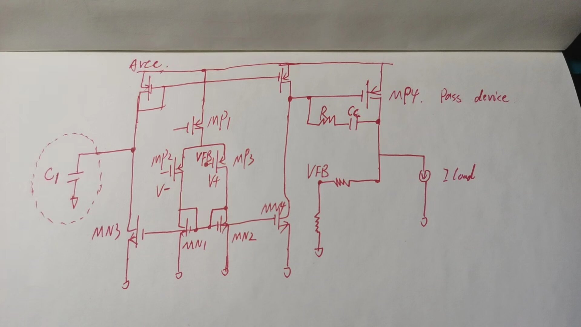
Hello, I have met a LDO circuit as shown, the first stage is a symmetric op and MP4 is the pass device. With cap C1 added, the PSR has significant improvement, but I'm confused on how to choose C1's Capacitance, I simulate it when C1 is too large or small, it has no effect. I simulate it with 1V ac on AVCC and plot output node‘s response. So, What's the principle of this method and how to choose C1?Is there any paper about it?
A.jpg
 
C1 "injects" AVCC-GND dV/dt current into the left hand leg.
If AVCC jumps up, then top rack current increases and that
helps pull the pass FET gate along for the ride. Somewhat.
Or over the top, depending on the "tune".

Now to me the circuit looks incomplete, the left side of the
diff pair has no signal indicated on its gate (that I can see)
for the VRef input. Also no bias for the bottom rack other
than the diff tail through-current and that "mirror" is malformed
(both sides D-G connected, so where's the current difference
supposed to come from?).

If pass FET is big then you probably need a buffer stage to get
decent load step response. The pass FET might "soak up" any
perturbation to the control amp. You can expect no help at low
supply frequency, this is a HF PSRR tweak "counter-injecting".
And such schemes help, until they hurt (a little more phase lag
in that "compensation" and you can pick up HF "whoop-de-do!"
artifacts which (you hope) something else will squash "adequately".

But adequate means different things to different people, like a
RF lineup might see that "whoop-de-do" as in-band amplified
switched harmonics mixing in.
Well, I redraw the sch. like this, the bias circuit is not shown. You mean with an ac disturbance on AVCC, there is a noise current on the left hand leg, and MP6 will copy this noise current to the right hand, which will inject to node M. And now the node M is a noisy node, which cancels AVCC's disturbance, and ultimately the output node is noise-free, and the PSR is improved. So if I choose a larger C1, the improvement will be more obvious? But through simulation I found it is no effect if C1 is too large or too small, there seems to be a relationship between C1 and Cc, if Cc increases, C1 should also be increased. Why is it not the larger C1 the better PSR?And the value of C1 could only be obtained by simulation, or rather, by sweeping the value of C1?
AA.jpg
 
The "tweak cap" is trying to "null" the output perturbation that
a supply-jump would make at the back end, by injecting an
opposing stimulus at the front end.

That can work but is a balancing act, if you keep increasing the
cap value expect to see a sag instead of a jump, on a positive-
going supply step.

Do a parameter loop and observe the family-of-curves for a
fixed VCC step, maybe the same on a PSRR Bode plot, if they
get to giving you the same story for cap value then great.

Until you start to look at temperature, tolerances, DC load
point and the yet-uninserted parasitics... because the two
paths share only a little commonality (basically the pass FET
and its too-wimpy drive buffer) and differ in phase lag with
forward-path-gain being pretty variable.

To me this is a "one trick pony" and you're really needing to
pull the whole wagon, rain or shine.
 
C1 has some effects. Here I inject a triangle ripple into Vdd.ac and square wave into Vin+ (Vref) with a gain of 2.
and give you sliders for each input and you can adjust C, RC with mouse slider.

All FETs are |Vt|= 1.5 Beta = 50m

good ruck.
 

LaTeX Commands Quick-Menu:

Part and Inventory Search

Welcome to EDABoard.com

Sponsor

Back
Top